background image

Getting Started

www.ti.com

2

SPRUIM4B – December 2018 – Revised May 2020

Submit Documentation Feedback

Copyright © 2018–2020, Texas Instruments Incorporated

xWR1843 Evaluation Module (xWR1843BOOST) Single-Chip mmWave
Sensing Solution

1

Getting Started

1.1

Introduction

The xWR1843 BoosterPack from Texas Instruments is an easy-to-use evaluation board for the xWR1843
mmWave sensing device, with direct connectivity to the microcontroller (MCU) LaunchPad Development
Kit. The BoosterPack contains everything required to start developing software for on-chip C67x DSP core
and low-power ARM R4F controllers, including onboard emulation for programming and debugging as well
as onboard buttons and LEDs for quick integration of a simple user interface.

The standard 20-pin BoosterPack headers make the device compatible with a wide variety of TI MCU
LaunchPads and enables easy prototyping.

1.2

Key Features

Two 20-pin LaundPad connectors that leverages the ecosystem of the TI LaunchPad

XDS110 based JTAG emulation with a serial port for onboard QSPI flash programming

Back-channel UART through USB-to-PC for logging purposes

Onboard antenna

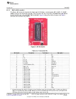
60-pin, high-density (HD) connector for raw analog-to-digital converter (ADC) data over LVDS and
trace-data capability

Onboard CAN-FD transceiver

One button and two LEDs for basic user interface

5-V power jack to power the board

1.3

Kit Contents

The following items are included with the xWR1843BOOST kit.

xWR1843 evaluation board

Mounting brackets, screws, and nuts to place the printed-circuit board (PCB) vertical

Micro USB cable to connect to PC

NOTE:

A 5-V, > 2.5-A supply brick with a 2.1-mm barrel jack (center positive) is not included. TI

recommends using an external power supply that complies with applicable regional safety
standards, such as UL, CSA, VDE, CCC, PSE, and more. The length of the power cable
should be < 3 m.

1.3.1

mmWave Proximity Demo

TI provides sample demo codes to easily get started with the xWR1843 evaluation module (EVM) and to
experience the functionality of the xWR1843 radar sensor. For details on getting started with these demos,
see

www.ti.com/tool/mmwave-sdk

.

Summary of Contents for WR1843 Series

Page 1: ...uttons and LEDs for quick integration of a simple user interface Contents 1 Getting Started 2 1 1 Introduction 2 1 2 Key Features 2 1 3 Kit Contents 2 2 Hardware 3 2 1 Block Diagram 5 2 2 Power Connections 5 2 3 Connectors 6 2 4 PC Connection 9 2 5 Connecting the BoosterPack to the DCA1000 9 2 6 Connecting the BoosterPack to the LaunchPad or the MMWAVE DEVPACK 10 2 7 Antenna 11 2 8 Jumpers Switche...

Page 2: ...em of the TI LaunchPad XDS110 based JTAG emulation with a serial port for onboard QSPI flash programming Back channel UART through USB to PC for logging purposes Onboard antenna 60 pin high density HD connector for raw analog to digital converter ADC data over LVDS and trace data capability Onboard CAN FD transceiver One button and two LEDs for basic user interface 5 V power jack to power the boar...

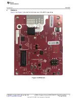
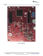
Page 3: ...0 Submit Documentation Feedback Copyright 2018 2020 Texas Instruments Incorporated xWR1843 Evaluation Module xWR1843BOOST Single Chip mmWave Sensing Solution 2 Hardware Figure 1 and Figure 2 show the front and rear view of the EVM respectively Figure 1 EVM Front ...

Page 4: ...om 4 SPRUIM4B December 2018 Revised May 2020 Submit Documentation Feedback Copyright 2018 2020 Texas Instruments Incorporated xWR1843 Evaluation Module xWR1843BOOST Single Chip mmWave Sensing Solution Figure 2 EVM Rear ...

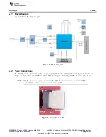
Page 5: ...gure 3 shows the block diagram Figure 3 Block Diagram 2 2 Power Connections The BoosterPack is powered by the 5 V power jack 2 5 A current limit shown in Figure 4 As soon as the power is provided the NRST and 5 V LEDs should glow indicating that the board is powered on NOTE After the 5 V power supply is provided to the EVM it is recommended to press the NRST switch SW2 one time to ensure a reliabl...

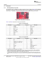
Page 6: ...T 11 WARMRST 12 SPI_MOSI 13 BSS LOGGER 14 SPI_MISO 15 SOP2 16 HOSTINT 17 SOP1 18 GPIO02 19 SOP0 20 NC 1 Voltage input to the GPADC available on the xWR1843 2 Indicates the state of the onboard VIO supply for the AWR device coming from the onboard PMIC A HIGH on the PGOOD signal 3 3 V indicates the supply is stable Because the I Os are not failsafe the MCU must not drive any I O signals to the AWR ...

Page 7: ...board VIO supply for the AWR device coming from the onboard PMIC A HIGH on the PGOOD signal 3 3 V indicates the supply is stable Because the I Os are not failsafe the MCU must not drive any I O signals to the AWR device before this I O supply is stable to avoid leakage current into the I Os Table 3 J1 Connector Pin Pin Number Description Pin Number Description 1 5V 2 5V 3 5V 4 TDO 5 TDI 6 TCK 7 SP...

Page 8: ...A15 50 LVDS_1P 51 I2C_SDA 52 LVDS_1M 53 I2C_SCL 54 GND 55 RS232RX Rx into AWR device 56 LVDS_0P 57 RS232TX Tx from AWR device 58 LVDS_0M 59 nRESET 60 GND 2 3 3 CAN Interface Connector The J3 connector provides the CAN_L and CAN_H signals from the onboard CAND FD transceiver TCAN1042HGVDRQ1 These signals can be directly wired to the CAN bus Because the digital CAN signals Tx and Rx are muxed with t...

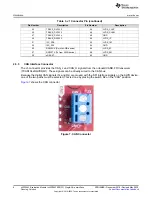
Page 9: ...on data sent through the UART MSS logger UART can be used to get MSS code logs on the PC When the USB is connected to the PC the device manager should recognize the following COM ports shown in Figure 8 XDS110 Class Application User UART UART1 port XDS110 Class Auxiliary Data Port MSS logger port Figure 8 COM Ports If Windows is unable to recognize the COM ports users must install the EMU pack ava...

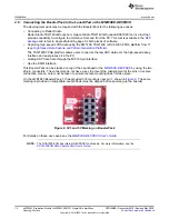
Page 10: ...peed Data Capture and Pattern Generation Platform The TSW1400 FPGA platform allows users to capture the raw ADC data over the high speed debug interface and post process it in the PC Getting DSP trace data through the MIPI 60 pin interface Use the DMM interface This BoosterPack can be stacked on top of the Launchpad or the MMWAVE DEVPACK by using the two 20 pin connectors The connectors do not hav...

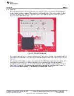
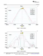
Page 11: ...ane Figure 10 shows the PCB antennas Figure 10 RX and TX Antennas The antenna peak gain is 10 5 dBi across the frequency band of 76 to 81 GHz The radiation pattern of the antenna in the horizontal plane H plane and elevation plane E plane is as shown in Figure 11 and Figure 12 The beamwidth of the antenna design can be determined from the radiation patterns For example at 78 GHz based on 3 dB drop...

Page 12: ...cember 2018 Revised May 2020 Submit Documentation Feedback Copyright 2018 2020 Texas Instruments Incorporated xWR1843 Evaluation Module xWR1843BOOST Single Chip mmWave Sensing Solution Figure 11 Antenna Pattern Figure 12 Antenna Pattern ...

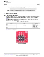
Page 13: ...the user and the EVM 2 8 Jumpers Switches and LEDs 2 8 1 Sense on Power SOP Jumpers The xWR1843 device can be set to operate in three different modes based on the state of the SOP lines These lines are sensed only during boot up of the AWR device The state of the device is detailed by Table 4 The SOP mode is set using switch S1 When the switch position is ON this refers to a 1 When the switch posi...

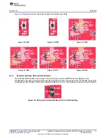
Page 14: ...le 5 provides the switch and LED information Table 5 Switch and LED Information Reference Usage Comments SW2 RESET Used to RESET the xWR1843 device This signal is also brought out on the 20 pin connector and 60 pin HD connector so an external processor can control the AWR device The onboard XDS110 can also use this reset SW1 GPIO_1 When pushed the GPIO_1 is pulled to VCC DS2 Warm reset indication ...

Page 15: ...Ds Figure 15 SW1 Figure 16 SW2 Figure 17 DS2 Figure 18 DS4 Figure 19 DS1 Figure 20 DS3 2 8 4 Selection Between SPI and CAN Interface The SPI and CAN interface are muxed on the same lines on the xWR1843 device Based on the configuration the user can select if the pins E14 and D13 must be connected to the 20 pin HD connectors to provide the SPI interface OR to the onboard CANFD PHY U3 This selection...

Page 16: ...ivalent capacitor in their designs 3 2 Software Development Tools and Example Code To enable quick development of end applications on the C67x DSP and R4F core in the xWR1843 TI provides a software development kit SDK that includes demo codes software drivers emulation packages for debug and more These can be found at mmwave sdk 3 2 1 LDO Bypass Requirement The xWR1843BOOST utilizes a 1 0 V supply...

Page 17: ...re Tools 17 SPRUIM4B December 2018 Revised May 2020 Submit Documentation Feedback Copyright 2018 2020 Texas Instruments Incorporated xWR1843 Evaluation Module xWR1843BOOST Single Chip mmWave Sensing Solution Figure 22 LDO Bypass Enable ...

Page 18: ... There could be small ringing behavior at the point of transient load change If this is impacting the RX sampled data the ADC start time can be increased to a point where the supply is settled within 5 or the inductance value can be reduced to reduce the ringing which may come at the expense or poorer 4 Mhz filtering 4 Design Revision History Table 6 Design Revision History PCB Revision Change Des...

Page 19: ...ation in open environments This oxidation causes the surface around the antenna region to blacken To avoid oxidation the PCB should be stored in an ESD cover and kept at a controlled room temperature with low humidity conditions All ESD precautions must be taken while using and handling the EVM 7 Troubleshooting EVM Board Power up Failure See Section 2 2 for desired power connections Please ensure...

Page 20: ...bmit Documentation Feedback Copyright 2018 2020 Texas Instruments Incorporated Revision History Revision History NOTE Page numbers for previous revisions may differ from page numbers in the current version Changes from A Revision August 2019 to B Revision Page Added Note 16 ...

Page 21: ...se resources are subject to change without notice TI grants you permission to use these resources only for development of an application that uses the TI products described in the resource Other reproduction and display of these resources is prohibited No license is granted to any other TI intellectual property right or to any third party intellectual property right TI disclaims responsibility for...

Reviews: