TOSHIBA
TMPR3904F Rev. 2.0
68
8.5.4
32/16-bit static bus sizing
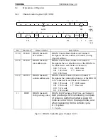
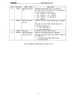
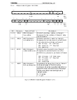
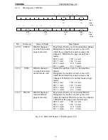
Supports the DRAM of 16-bit bus width by setting up 16BUS0 and 16BUS1 of the DCCRn
(n=1,0).
32-bit Bus Access
Indicates that the DRAM connected to the channel is 32-bit bus when the 16BUSn of the
DRAM channel control register is 0. It can conduct the most efficient memory access.
Word/triple-byte access with 16-bit width DRAM
Indicates that the DRAM connected to the channel is 16-bit bus when the 16BUSn of the
DRAM channel control register is 1. At this time, the DRAMC conducts a memory access twice
at the timing set up in the register when a word or triple-byte access is requested. The second
access shall be page mode.
Half-word/byte access with 16-bit width DRAM
If a half-word or byte access is requested when the 16BUSn of the DRAM channel control
register is 1, the DRAMC conducts a memory access once at the timing set up in the register.
8.5.5
Support for external bus master
In the TX3904, the DRAM memory address is multiplexed with the address bus signal. When
the external bus master conducts a memory access using the DRAMC, it is necessary to avoid
conflicts between the DRAM memory address output and the address signal that is output by the
external bus master.
The external bus master is expected to manage not to generate a page hit miss when it uses the
DRAMC. The accessing address must be word (32-bit) boundary. The number of data transfer
in burst mode must be a multiple of 32 bits.
8.5.6
Support for half speed bus
The signals generated for DRAM (address, data, RAS* and CAS*) is synchronized to a rising
edge of a processor clock (internal clock) in half speed bus mode. So these signals are not
synchronized to a rising edge of the SYSCLK.
When the external bus master conducts a memory access through the DRAMC in the half speed
mode, set up a wait in the DRAMC channel control register such that the number of the DRAM
access cycles (the number of GCLK cycles) is an even number.
Summary of Contents for TMPR3904F
Page 1: ...Users Manual 32bit RISC Microprocessor TX39 family TMPR3904F Rev 2 0 Jan 12 1998 ...
Page 2: ......
Page 9: ...Users Manual 01 1 INTRODUCTION 1 1 Overview ...
Page 11: ...Users Manual 03 1 3 Kind of accessing by the TX3904 ...
Page 12: ...Users Manual 04 1 4 Precautions in the TMPR3904F specification Don t set Don t use ...
Page 13: ...Users Manual 05 Do not use ...
Page 14: ...Users Manual 06 ...
Page 15: ...Users Manual 7 2 FEATURES n n n n n n n n n n n n n ...
Page 16: ...Users Manual 8 ...
Page 18: ...Users Manual 10 ...
Page 19: ...Users Manual 11 4 PINS 4 1 Positions of Pins ...
Page 20: ...Users Manual 12 ...
Page 21: ...Users Manual 13 4 2 Functions of Pins ...
Page 22: ...Users Manual 14 ...
Page 23: ...Users Manual 15 ...
Page 24: ...Users Manual 16 ...
Page 26: ...Users Manual 18 5 2 Register Map ...
Page 27: ...Users Manual 19 ...
Page 28: ...Users Manual 20 ...
Page 30: ...Users Manual 22 5 3 2 PIO2 and PIO1 ...
Page 32: ...Users Manual 24 5 3 4 Connection of external bus master 5 3 5 INT 7 0 active status clear ...
Page 33: ...Users Manual 25 5 3 6 INT 7 0 active status set up ...
Page 34: ...Users Manual 26 ...
Page 123: ...TOSHIBA TMPR3904F Rev 2 0 115 26 ...
Page 169: ...TOSHIBA TMPR3904F Rev 2 0 161 26 ...
Page 203: ...TOSHIBA TMPR3904F Rev 2 0 195 ...
Page 230: ......

