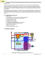
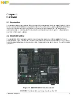
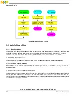
background image

MC9S12
Microcontrollers

freescale.com

Designer Reference Manual

USB2.0 Card Reader

DRM065
Rev. 0.1
01/2005

Summary of Contents for MC9S12

Page 1: ...MC9S12 Microcontrollers freescale com Designer Reference Manual USB2 0 Card Reader DRM065 Rev 0 1 01 2005 ...

Page 2: ......

Page 3: ... of our documents on the World Wide Web will be the most current Your printed copy may be an earlier revision To verify that you have the latest information available refer to http www freescale com The following revision history table summarizes changes contained in this document For your convenience the page number designators have been linked to the appropriate location Revision History Date Re...

Page 4: ...Revision History MC9S12UF32 Card Reader Reference Design User Manual Rev 0 1 4 Freescale Semiconductor ...

Page 5: ...4 3 USB Interface 9 1 4 4 Memory Cards Interfaces 9 Chapter 2 Hardware 2 1 Introduction 11 2 2 M68EVB912UF32 11 2 3 Modifications 12 Chapter 3 Software Overview 3 1 System Software Architecture 13 3 2 Main Software Flow 14 3 2 1 Main Program 14 3 2 1 1 USB Events Handler 14 3 2 1 2 USBMS Events Handler 14 3 2 1 3 Card Insertion and Removal Handler 14 3 2 2 Timer Interrupt 15 3 2 3 USB Interrupts 1...

Page 6: ...lock Wrapper 25 6 3 1 1 Commands Without Data Transfer 26 6 3 1 2 Host Sends out Data to Storage Device 26 6 3 1 3 Host Receives Data from Storage Device 26 6 3 2 Class Specific Request 28 Chapter 7 Memory Cards Mass Storage Drivers 7 1 Introduction 29 7 2 RAM Mapping 29 7 3 Windows File Systems and MS SM Data Format 29 7 4 Memory Card Mass Storage Drivers 31 7 4 1 Commands Without Data Transfer 3...

Page 7: ... Magic Gate Secure Digital MultimediaCard SmartMedia 1 3 MC9S12UF32 Features The MC9S12UF32 microcontroller hereafter referred as UF32 features an integrated Universal Serial Bus USB 2 0 controller and physical layer transceivers to provide comprehensive USB specification implementation for both high speed 480 Mbps and full speed 12 Mbps operations The high speed operation running at bus speed of ...

Page 8: ...while the 64 pin device is designed for ATA ATAPI bridge with SD access or USB applications with SM SD and MS access and other USB applications that do not require so many I O pins 1 3 1 MC9S12UF32 feature List HCS12 core 32K Bytes Flash 3 5K Bytes RAM 1 5K Bytes Queue RAM Universal Serial Bus 2 0 controller and transceivers Integrated Queue controller ATA ATAPI Host controller CompactFlash Host c...

Page 9: ... I O The UF32 has got four built in regulators 2 5V regulator for S12 core use 2 5V regulator for USB transceiver use 3 3V regulator for USB transceiver and PLL use 3 3V regulator that needed an external MOSFET The S12 core is powered by the internal 2 5V regulator The USB transceivers and PLL is powered by the internal 3 3V regulator The UF32 needs a 5V power supplied to VDDR The external MOSFET ...

Page 10: ...System Overview MC9S12UF32 Card Reader Reference Design User Manual Rev 0 1 10 Freescale Semiconductor ...

Page 11: ...hematics of the board for detail operations The board was not optimized design for a card reader To implement a card reader customer may refer to the schematic provided in this reference design 2 2 M68EVB912UF32 The M68EVB912UF32 evaluation platform board hereafter referred as EVB consists of a 100 pin package UF32 a 12V to 5V DC DC converter a RS 232 transceiver and some other glue logics It has ...

Page 12: ... 3V and to connect the card detection pins to the UF32 Figure 2 2 Modifications Connections Figure 2 2 shows the modifications required Short CR5 to bypass the diode needed for EVB of revision 5 or older version Short W19 pin 1 2 and 3 Connect JP10 pin 5 and JP9 pin 4 for CompactFlash card detection Connect JP16 pin 12 and JP9 pin 5 for Secure Digital card detection Connect JP16 pin 14 and JP9 pin...

Page 13: ...for multi tasks operation In this application it mainly handles the USB event tasks and the timer hook function tasks after system initialization The initialization subroutines initialize the modules of Timer Voltage Regulator IQUEUE RAM IQUEUE and USB Controller The main program continually checks and serves different event tasks The memory card host controller will be initialized after the card ...

Page 14: ...r The USB Events Handler handles the USB Mass Storage reset and the USB Mass Storage Command Block Wrapper 3 2 1 3 Card Insertion and Removal Handler The card insertion and removal handler checks any card inserted or removed from the sockets for every 100ms The time interval is defined in the timer hook function If any card is detected to be inserted the handler will enable and initialize the card...

Page 15: ...terrupts for the control Endpoint 0 Interrupts for the Bulk IN Endpoint Interrupts for the Bulk OUT Endpoint All of the interrupt events are fully handled in the interrupt routines excepts the following interrupts USB suspend USB Mass Storage reset USB Mass Storage Command Block Wrapper received The above 3 interrupt routines set some flags to indicate their presents and will then be served in the...

Page 16: ...Software Overview MC9S12UF32 Card Reader Reference Design User Manual Rev 0 1 16 Freescale Semiconductor ...

Page 17: ...be mapped to the logical endpoints 1 to 3 However only one logical endpoint can be mapped to the logical endpoints 3 The maximum buffer sizes of endpoints 4 and 5 are 64 bytes at USB full speed or 512 bytes at high speed IQUEUE RAM is used as the buffers for these two endpoints The other endpoints are associated with delicate 64 bytes of buffers In this application only the control endpoints and t...

Page 18: ... modules include enabling the 480MHz PLL and the necessary USB Endpoint 0 Interrupts and setting the card reader as self or bus powered The external USB 1 5K pullup resistor is then configured to be connected to the USB D pin through the UF32 After detecting the pullup at the D pin the host will send out a USB Reset signal to the UF32 The USB module Status Register will indicate whether the commun...

Page 19: ...e configured to transfer data to and from different peripherals QC1 is with the highest priority while QC4 is with the least priority QC1 and QC2 QC3 and QC4 can be configured as two double buffer channels For IQUEUE module to transfer data from one peripheral to another automatically a single or double buffers channel with passing through mode must be used For proper operation the USB peripheral ...

Page 20: ...e 5 1 IQUEUE Request Mapping Data Flow QCnREQ Peripheral Functions Direction PC USB QRAM QC1REQ 0 USB Rx PC USB QRAM QC3REQ 1 USB Tx QRAM CF QC4REQ 4 CF Rx QRAM CF QC2REQ 5 CF Tx QRAM MS QC4REQ 6 MS Rx QRAM MS QC2REQ 7 MS Tx QRAM SD QC4REQ 8 SD Rx QRAM SD QC2REQ 9 SD Tx QRAM SM QC4REQ 10 SM Rx QRAM SM QC2REQ 11 SM Tx ...

Page 21: ... The subclass of the SCSI Transparent command 0x06 is used since the SCSI command can support most storage and multimedia devices 6 2 USB Mass Storage Class Bulk Only Transport In Bulk Only Transport the transfer of command data and status occurring solely via Bulk endpoints There are two class specific requests through the SETUP command Bulk Only Mass Storage Reset Get Max LUN The Bulk Only Mass ...

Page 22: ...ode of 0x06 of the SCSI Transparent Command Set Table 6 1 Command Block Wrapper bit Byte 7 6 5 4 3 2 21 0 0 3 LSB Byte 0 MSB Byte 3 dCBWSignature 0x55 0x53 0x42 0x43 4 7 dCBWTag 8 11 dCBWDataTransferLength number of bytes of data transfer expected 12 bmCBWFlags 13 Reserved 0 bCBWLUN logical device number 14 Reserved 0 bCBWCBLength Command Block length 15 30 bCBWCB Command Block READY HOST SENDS OU...

Page 23: ... its last byte For any command if there is an invalid parameter in the CDB the target should terminate the command without altering the medium Table 6 2 Command Status Wrapper 7 6 5 4 3 2 21 0 0 3 dCSWSignature 0x55 0x53 0x42 0x53 4 7 dCSWTag get from the CBW 8 11 dCSWDataResidule number of bytes different between expected transfer length and actual handled 12 bmCSWStatus Table 6 3 CDB of 6 byte C...

Page 24: ...6 5 4 3 2 21 0 0 Operation Code 1 Reserved 0 Service Action if required 2 5 MSB byte 2 Logical Block Address if required LSB byte 5 6 9 MSB byte 6 Additional CDB Data if required LSB byte 9 10 13 MSB byte 10 LSB byte 13 Transfer Length if required Parameter List Length if required Allocation length if required 14 Reserved 15 Control Table 6 7 CDB of long LBA 16 byte Command 7 6 5 4 3 2 21 0 0 Oper...

Page 25: ...e device require host to receive data from storage device After decoding the SCSI command from the CBW the driver will either handle the command without interfere with the individual storage device driver or translate the command and call individual routines of the storage device driver After receiving a 31 byte CBW and all data has been transferred the UF32 will return a 13 byte CSW to the host w...

Page 26: ...ceives all the data from host and sends all the data to the storage it will check whether the device has successfully received the data without any error 6 3 1 3 Host Receives Data from Storage Device After sending out a 31 byte CBW the host expects the storage device to send out data If an error happens and the host has not acknowledged ACK all the data from the device a zero length data will be ...

Page 27: ... RETURNS CSW YES SCSI COMMAND HANDLING NO DATA TRANSFER IS EXPECTED HOST TO RECEIVE DATA FROM DEVICE HOST TO SEND DATA TO DEVICE COMMAND SUPPORTED COMMAND SUPPORTED COMMAND SUPPORTED STALL STALL IN STALL OUT ENDPOINT gUSBCSWResult Failed gUSBCSWResult Failed IN DATAx DATA RETURNS ZERO ERROR FOUND LENGTH DATA DATA COMMAND SUCCESS gUSBCSWResult Failed COMMAND SUCCESS gUSBCSWResult Failed YES YES NO ...

Page 28: ... value from 0 to 15 representing a logical unit number 1 to 16 After receiving the Bulk Only Mass Storage Reset the driver calls the reset routines of the registered storage devices one by one The driver returns STALL to other reserved class specific reqests Figure 6 4 Software Flow of Class Specific Request SETUP DATA0 8 BYTE CBW GET MAX LUN IN DATAx 1 BYTE LUN DEVICE RETURNS LUN HOST SENDS OUT b...

Page 29: ...ical segment 0 of the card which is to store boot record FAT table and directories contents The RAM block 1 is to store the conversion table for other physical segments of the card 7 3 Windows File Systems and MS SM Data Format Windows File Systems use the concept of sector and cluster to store data A sector size is a multiple of 512 bytes and is usually 512 bytes for memory cards A cluster repres...

Page 30: ...ster 3 with logical block addresses from 96 to 127 S e c to r 5 1 2B y te s C lu s te r 2 NS e c to r F A TS y s te m P a g e 5 1 2 1 6B y te s B lo c k 1 6o r3 2P a g e s M So rS M S e c to r 5 1 2B y te s C lu s te r 2 NS e c to r F A TS y s te m P a g e 5 1 2 1 6B y te s B lo c k 1 6o r3 2P a g e s M So rS M P a g e0 P a g e1 P a g e2 P a g e1 4 3 0 P a g e1 5 3 1 2 5 6B y teD a ta2 5B y te sR ...

Page 31: ... write command is supported in which host writes data into card Figure 7 4 shows the software flow After sending out the CBW the host sends out data of the corresponding LBA to the card reader For MS and SM the driver gets the LBA and determines its corresponding segment The logical to physical table LogToPhyTbl is updated if necessary The PBA is then retrieved from the LogToPhyTbl The data is wri...

Page 32: ...eturns mode sense data Read Capacity card reader returns total capacity to host Read Packet card reader returns data to host by setting up the IQUEUE channels Figure 7 5 shows the flow of the SCSI command read packet The data of the corresponding LBA will be sent to host once the UF32 received the SCSI read command The logical to physical block address translation is needed for SM and MS only SCSI...

Page 33: ...ce Design User Manual Rev 0 1 Freescale Semiconductor 33 Figure 7 5 SCSI Command Read Packet SCSI Command Read_10 Get LBA Update LogToPhyTbl if necessary Decode LBA to PBA Get data from Card LBA Send out data to host via IQUEU Finish reading all LBAs NO YES RETURN ...

Page 34: ...Memory Cards Mass Storage Drivers MC9S12UF32 Card Reader Reference Design User Manual Rev 0 1 34 Freescale Semiconductor ...

Page 35: ... To implement a card reader the customer may refer to the schematic provided in this reference design 8 2 2 Firmware There are two projects created One is UF32 Card Reader CW v31 mcp card reader project under the application directory Another is the UF32Kernel_Lib mcp mini kernel project under the UF32 Kernel_Lib directory 8 2 2 1 UF32 Card Reader Project There are two targets of Development and C...

Page 36: ...Testing and Customization MC9S12UF32 Card Reader Reference Design User Manual Rev 0 1 36 Freescale Semiconductor ...

Page 37: ...it ALU The portion of the CPU that contains the logic circuitry to perform arithmetic logic and manipulation operations on operands asynchronous Refers to logic circuits and operations that are not synchronized by a common reference signal ATD See analogue to digital converter B See accumulators A and B or D baud rate The total number of bits transmitted per unit of time BCD See binary coded decim...

Page 38: ...M clear To change a bit from logic 1 to logic 0 the opposite of set clock A square wave signal used to synchronize events in a computer clock generator module CGM The CGM module generates a base clock signal from which the system clocks are derived The CGM may include a crystal oscillator circuit and or phase locked loop PLL circuit comparator A device that compares the magnitude of two inputs A d...

Page 39: ...registers in an M68HC12 are A 8 bit accumulator B 8 bit accumulator D 16 bit accumulator formed by concatenation of accumulators A and B IX 16 bit index register IY 16 bit index register SP 16 bit stack pointer PC 16 bit program counter CCR 8 bit condition code register cycle time The period of the operating frequency tCYC 1 fOP D See accumulators A and B or D decimal number system Base 10 numberi...

Page 40: ...erve as a temporary data storage locations input output I O Input output interfaces between a computer system and the external world A CPU reads an input to sense the level of an external signal and writes to an output to change the level on an external signal instructions Operations that a CPU can perform Instructions are expressed by programmers as assembly language mnemonics A CPU interprets an...

Page 41: ...s is a serial communications protocol which supports distributed real time control efficiently and with a high degree of noise immunity microcontroller Microcontroller unit MCU A complete computer system including a CPU memory a clock oscillator and input output I O on a single integrated circuit modulo counter A counter that can be programmed to count to any number from zero to its maximum possib...

Page 42: ...inds a byte with an incorrect number of logic 1s PC See program counter PC peripheral A circuit not under direct CPU control phase locked loop PLL A clock generator circuit in which a voltage controlled oscillator produces an oscillation which is synchronized to a reference signal PLL See phase locked loop PLL pointer Pointer register An index register is sometimes called a pointer register becaus...

Page 43: ...o a known condition SCI See serial communication interface module SCI serial Pertaining to sequential transmission over a single line serial communications interface module SCI A module that supports asynchronous communication serial peripheral interface module SPI A module that supports synchronous communication set To change a bit from logic 0 to logic 1 opposite of clear shift register A chain ...

Page 44: ... PLL operation with narrow loop bandwidth Also see acquisition mode two s complement A means of performing binary subtraction using addition techniques The most significant bit of a two s complement number indicates the sign of the number 1 indicates negative The two s complement negative of a number is obtained by inverting each bit in the number and then adding 1 to the result unbuffered Utilize...

Page 45: ......

Page 46: ...y of its products for any particular purpose nor does Freescale Semiconductor assume any liability arising out of the application or use of any product or circuit and specifically disclaims any and all liability including without limitation consequential or incidental damages Typical parameters that may be provided in Freescale Semiconductor data sheets and or specifications can and do vary in dif...

Reviews: