Page 5-3
Manual MPCI-ICM4S.F1b
The second initializing step is to set the Line Control Register at Base A3. This register
defines word length, stop bits, parity, and the DLAB.
Bits 0 and 1 control word length and allow word lengths from 5 to 8 bits. Bit settings are
extracted by subtracting 5 from the desired word length.
Bit 2 determines the number of stop bits. There can be either one or two stop bits. If Bit 2 is
set to 0, there will be one stop bit. If Bit 2 is set to 1, there will be two.
Bits 3 through 6 control parity and break enable. They are not commonly used for
communications and should be set to zeroes.
Bit 7 is the DLAB discussed earlier. It must be set to zero after the divisor is loaded or else
there will be no communications.
The C command to set the UART for an 8-bit word, no parity, and one stop bit is:
outportb(BA3, 0x03)
The final initialization step is to flush the receiver buffers. You do this with two reads from the
receiver buffer at base a0. When done, the UART is ready to use.
Reception
Reception can be handled in two ways: polling or interrupt-driven. When polling, reception is
accomplished by constantly reading the Line Status Register at Base A5. Bit 0 of this
register is set high whenever data are ready to be read from the chip. A simple polling loop must
continuously check this bit and read in data as it becomes available. The following code fragment
implements a polling loop and uses a value of 13, (ASCII Carriage Return) as an end-of-transmission
marker:
do
{
while (!(inportb(BA5) & 1)); /*Wait until data ready*/
data[i++]= inportb(BASEADDR);
}
while (data[i]!=13);
/*Reads the line until null character rec'd*/
Interrupt-driven communications should be used whenever possible and is required for high data
rates. Writing an interrupt-driven receiver is not much more complex than writing a polled receiver
but care should be taken when installing or removing your interrupt handler to avoid writing the
wrong interrupt, disabling the wrong interrupt, or turning interrupts off for too long a period.
Summary of Contents for PCI-ICM422/2
Page 2: ......
Page 16: ...PCI ICM422 2 4 and 485 2 4 Manual Page 2 6 Manual MPCI ICM4S F1b...
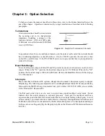
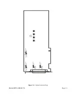
Page 19: ...Page 3 3 Manual MPCI ICM4S F1b Figure 3 2 Option Selection Map...
Page 20: ...PCI ICM422 2 4 and 485 2 4 Manual Page 3 4 Manual MPCI ICM4S F1b...
Page 22: ...PCI ICM422 2 4 and 485 2 4 Manual Page 4 2 Manual MPCI ICM4S F1b...
Page 28: ...PCI ICM422 2 4 and 485 2 4 Manual Page 6 2 Manual MPCI ICM4S F1b...
Page 32: ...PCI ICM422 2 4 and 485 2 4 Manual Page A 4 Manual MPCI ICM4S F1b...


