background image


4.0    GPIO & Delay Time Setting  


4.1    GPIO and Ignition Control Register


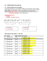
The General Purpose I/O is an interface available on some devices. These can read  
digital signals from other parts of a circuit, or output to control other devices. At GPIO 
control register, the GPI is use to receive data, the GPO is set data to send. 


I/O port: 

0xA35 (base address)


for Control Register (Read 0xA2h / Write 0xA1h)


0xA36 (base address) 

for Control Data Value 


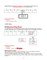
Debug Command Line


O A35 A1 


O A36 0F  // Set Bit 4-7 to Low 


7


6


5


4


3


2


1


0


DO4 

DO3 

DO2 

DO1 

DI4 

DI3 

DI2 

DI1 


0 = DO is low 


0 = DI is low *


1 = DO is high *


1 = DI is high 


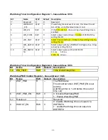
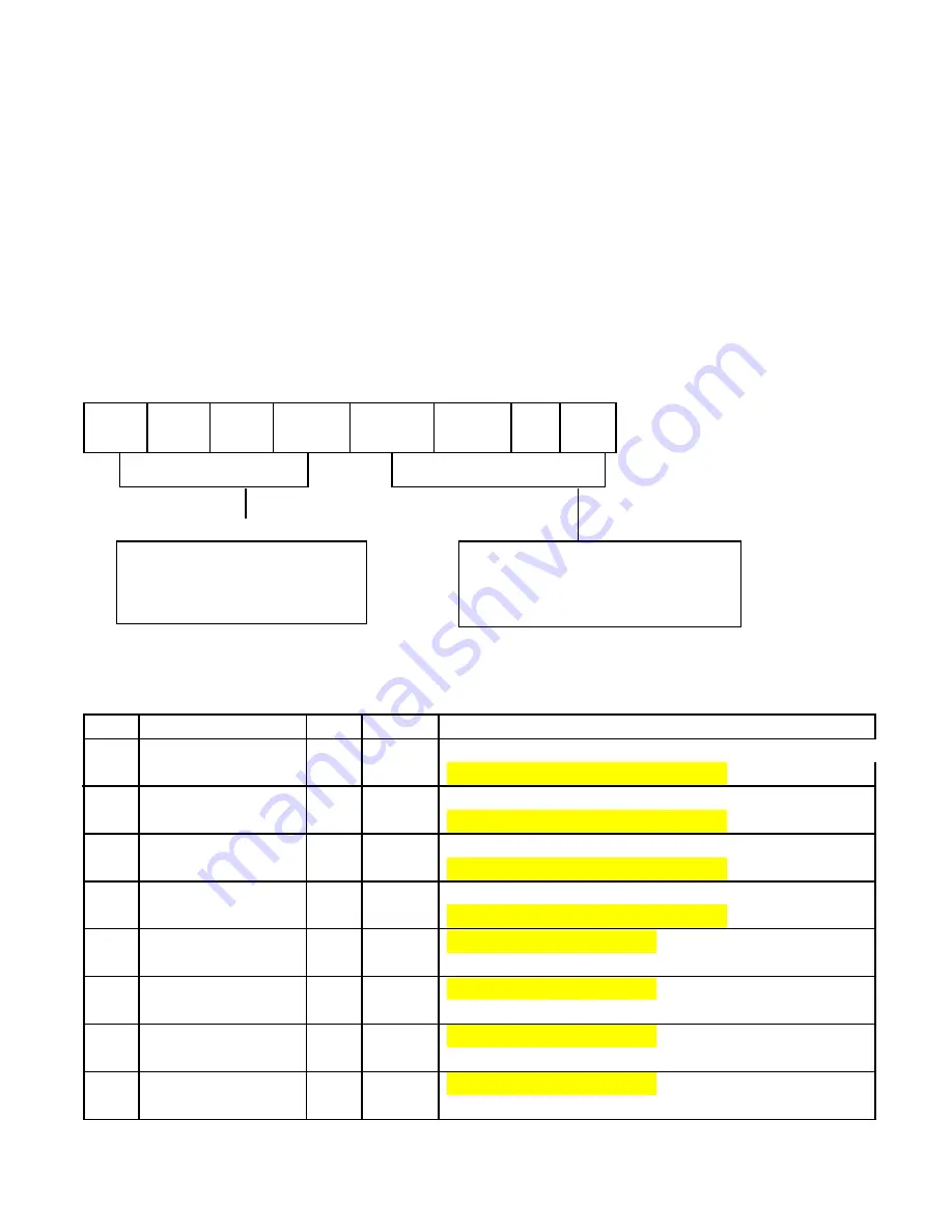
PIO5 Output Enable Register – Index A0h 


Bit


Name


R/W


Default


Description


7  

GPIO57_OE 

R/W 

  0 : GPIO57 is input                                                      


  1 : GPIO57 is output 


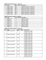
6  

GPIO56_OE 

R/W 

  0 : GPIO56 is input 


  1 : GPIO56 is output 


5  

GPIO55_OE 

R/W 

  0 : GPIO55 is input 


  1 : GPIO55 is output 


4  

GPIO54_OE 

R/W 

  0 : GPIO54 is input 


  1 : GPIO54 is output 


3  

GPIO53_OE 

R/W 

  0 : GPIO53 is input 


  1 : GPIO53 is output 


2  

GPIO52_OE 

R/W 

  0 : GPIO52 is input 


  1 : GPIO52 is output 


1  

GPIO51_OE 

R/W 

  0 : GPIO51 is input 


  1 : GPIO51 is output 


0  

GPIO50_OE 

R/W 

  0 : GPIO50 is input 


Summary of Contents for PowerBrick 5.0

Page 1: ...PowerBrick 5 0 User s Manual Edition 2 0 3 Generation Intel i7 Industrial Computer Acura Embedded Systems Inc...

Page 2: ...Specification 4 2 1 VGA Connector 4 2 2 GPIO Connector 4 2 3 COM Port Connector 5 2 4 Power Input Connector 5 2 5 ATX 6PIN Connector POWER OUT 6 3 0 Ignition Power Management 6 4 0 GPIO Delay Time Se...

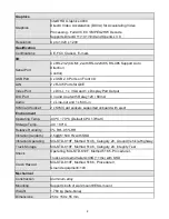
Page 3: ...2 HD Codec onboard Watchdog Watchdog Timer Support Offer 1 255 Step Power Requirement Power Input 9V 32V DC Power input Power Protection Automatics Recovery Short Circuit Protection Power Management V...

Page 4: ...80mA Audio 1 x Line out and 1 x MIC in SIM Card Socket 2 x SIM Card sockets supported onboard with eject Environment Operating Temp 40 C 70 C Default CPU 17Watt Storage Temp 40 80 C Relative Humidity...

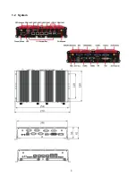
Page 5: ...1 2 System 3...

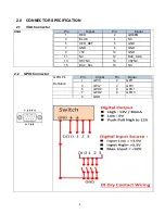
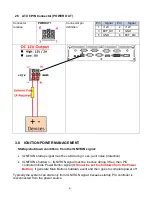
Page 6: ...nal Pin Signal 1 RED 2 GREEN 3 BLUE 4 NC 5 CER_DET 6 GND 7 GND 8 GND 9 5V 10 GND 11 NC 12 DAC_SDA 13 HSYNC 14 VSYNC 15 DAC_SCL 16 NC 2 2 GPIO Connector GPIO Pin Definition Pin Signal Pin Signal 1 GPI0...

Page 7: ...1 COM1 2 3 4_DCD COM1 2_RS 485_TXD RXD 2 COM1 2 3 4_RXD Com1 2_RS 485_TXD RXD 3 COM_TXD 4 COM_DTR 5 GND 6 COM_DSR 7 COM_RTS 8 COM_CTS 9 COM_RI 2 4 Power Input Connector PWRIN1 Connector definition Pin...

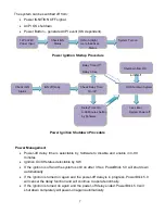
Page 8: ...NITION startup signal must be valid during 3 sec anti noise protection IGNITION shutdown IGNITION signal must be inactive during 3 Sec then PIC controller initiate Power Button signal OS must be set t...

Page 9: ...able in 0 99 minutes Ignition On Off status detectable by SW If the ignition is off and the system is still on after 3 Sec PowerBrick 5 0 will shut down automatically If the ignition is turned on agai...

Page 10: ...and Line O A35 A1 O A36 0F Set Bit 4 7 to Low 7 6 5 4 3 2 1 0 DO4 DO3 DO2 DO1 DI4 DI3 DI2 DI1 0 DO is low 0 DI is low 1 DO is high 1 DI is high PIO5 Output Enable Register Index A0h Bit Name R W Defau...

Page 11: ...n status 3 GPIO53_ST R 1 GPIO53 pin status 2 GPIO52_ST R 1 GPIO52 pin status 1 GPIO51_ST R 1 GPIO51 pin status 0 GPIO50_ST R 1 GPIO50 pin status GPIO5 Drive Enable Register Index A3h Bit Name R W Defa...

Page 12: ...nfiguration Port The following table describes the Control Register bit definition 7 6 5 4 3 2 1 0 0 0 1 1 Timer 0 Select output Unit pulse width of RSTOUT 0 1 sec 00 1 ms 1 60 sec 01 25 ms 10 125 ms...

Page 13: ...lect output polarity of RETOUT 1 high active 0 low active by setting the bit 1 0 WD_PSWID TH R W 0 Select output pulse width of RSTOUT 0 1 ms 1 25 ms 2 125 ms 3 5 sec Watchdog Timer Configuration Regi...

Page 14: ...5 0 BIOS Setting Super IO Configuration Select Serial Port Mode 12...

Page 15: ...ce A special customer service unit has been set up specifically to cater to our esteemed customers needs Technical Support For technical support contact your Salesperson support acuraembedded com Mail...

Reviews: