background image

Chapter 2: Getting Started with the Stratix V Hard IP for PCI Express

2–17

Quartus II Compilation

June 2012

Altera Corporation

Stratix V Hard IP for PCI Express

User Guide

2. Click the 

Generate

 button at the bottom of the 

Generation

 tab to create the 

chaining DMA simulation model, which you can include in your custom 
testbench.

1

You can generate the testbench which shows you the connections necessary between 
the Endpoint and a Root Port BFM. However, the BFM is not available for simulation 
in the current release.

Quartus II Compilation

This section provides step-by-step instructions for Quartus II compilation. To compile 
your Endpoint and design example, complete the instructions in one of the following 
two sections:

Compiling the Design in the MegaWizard Plug-In Manager Design Flow

Compiling the Design in the Qsys Design Flow

Compiling the Design in the MegaWizard Plug-In Manager Design Flow

Before compiling the complete example design in the Quartus II software, you must 
add the example design files that you generated in Qsys to your Quartus II project. 

Follow these steps to add the Quartus II IP File (

.qip

)


to the project:

1. On the Project menu, select 

Add/Remove Files in Project

2. Click the browse button next the 

File name

 box and browse to the 

gen1_x8_example_design/altera_pcie_sv_hip_ast/pcie_de_gen1_x8_ast128/
synthesis/ 

directory.

3. In the 

Files of type

 list

 pcie_de_gen1_x8_ast128.qip

 and then click 

Open

.

4. On the 

Add Files

 page, click 

Add

, then click 

OK

.

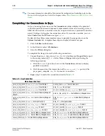
Synthesis

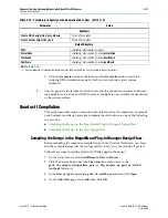
Create HDL design files for synthesis

Turn on this option

Create block symbol file (.bsf)

Turn on this option

Output Directory

Path

<

working_dir

>/

<variant_name>

Simulation

<

working_dir

>/

<variant_name>

/simulation 

Testbench 

<

working_dir

>/

<variant_name>

/testbench

Synthesis 

<

working_dir

>/

<variant_name>

/synthesis

Note to 

Table 2–15

:

(1) You can generate a simulation testbench; however the Root Port BFM is not available in the current release.

Table 2–15. Parameters to Specify on the Generation Tab in Qsys  (Part 2 of 2)

Parameter

Value

Summary of Contents for Stratix V Hard IP

Page 1: ...www altera com UG 01097 1 2 User Guide Stratix V Hard IP for PCI Express Document last updated for Altera Complete Design Suite version Document publication date 12 0 June 2012 Feedback Subscribe Stratix V Hard IP for PCI Express User Guide ...

Page 2: ...ductor products to current specifications in accordance with Altera s standard warranty but reserves the right to make changes to any products and services at any time without notice Altera assumes no responsibility or liability arising out of the application or use of any information product or service described herein except as expressly agreed to in writing by Altera Altera customers are advise...

Page 3: ...lation Model Using Qsys 2 16 Quartus II Compilation 2 17 Compiling the Design in the MegaWizard Plug In Manager Design Flow 2 17 Compiling the Design in the Qsys Design Flow 2 18 Modifying the Example Design 2 20 Chapter 3 Getting Started with the Avalon MM Stratix V Hard IP for PCI Express Creating a Quartus II Project 3 3 Running Qsys 3 4 Customizing the Avalon MM Stratix V Hard IP for PCI Expre...

Page 4: ...letions 5 14 PCI Express to Avalon MM Downstream Write Requests 5 14 PCI Express to Avalon MM Downstream Read Requests 5 15 Avalon MM to PCI Express Read Completions 5 15 PCI Express to Avalon MM Address Translation 5 15 Avalon MM to PCI Express Address Translation 5 16 Completer Only Single Dword Endpoint 5 17 RX Block 5 18 Avalon MM RX Master Block 5 19 TX Block 5 19 Interrupt Handler Block 5 19...

Page 5: ...r Interface Signals 6 52 Transceiver Reconfiguration 6 53 Serial Interface Signals 6 54 Channel Placement for Gen1 and Gen2 Using CMU PLL 6 54 Channel Placement for Gen1 and Gen2 Using ATX PLL 6 57 Channel Placement for Gen3 Using Both CMU and ATX PLLs 6 59 PIPE Interface Signals 6 59 Test Signals 6 62 Chapter 7 Register Descriptions Configuration Space Register Content 7 1 Altera Defined Vendor S...

Page 6: ...valon MM Interrupts 11 7 Chapter 12 Flow Control Throughput of Posted Writes 12 1 Throughput of Non Posted Reads 12 3 Chapter 13 Error Handling Physical Layer Errors 13 2 Data Link Layer Errors 13 2 Transaction Layer Errors 13 3 Error Reporting and Data Poisoning 13 5 Uncorrectable and Correctable Error Status Bits 13 6 Chapter 14 Hard IP Reconfiguration and Transceiver Reconfiguration Hard IP Rec...

Page 7: ...Chapter 1 vii June 2012 Altera Corporation Stratix V Hard IP for PCI Express User Guide How to Contact Altera Info 3 Typographic Conventions Info 3 ...

Page 8: ...1 viii Chapter Stratix V Hard IP for PCI Express June 2012 Altera Corporation User Guide ...

Page 9: ...ions Table 1 1 shows the aggregate bandwidth of a PCI Express link for Gen1 Gen2 and Gen3 for 1 4 and 8 lanes The protocol specifies 2 5 giga transfers per second for Gen1 5 giga transfers per second for Gen2 and 8 0 giga transfers per second for Gen3 Table 1 1 provides bandwidths for a single transmit TX or receive RX channel so that the numbers in Table 1 1 double for duplex operation Gen1 and G...

Page 10: ...sy to use Easy parameterization Substantial on chip resource savings and guaranteed timing closure Easy adoption with no license requirement Example designs to get started New features in the 12 0 release Avalon MM single dword variant saves resources for Endpoints performing simple reads and writes in response to Host CPU Gen3 Programmer Object File pof support for Stratix V production devices Ge...

Page 11: ...orted Qsys design flow Supported Supported 64 bit Application Layer interface Supported Supported 128 bit Application Layer interface Supported Supported 256 bit Application Layer interface Supported Not supported Transaction Layer Packet type TLP 5 Memory Read Request Memory Read Request Locked Memory Write Request I O Read Request I O Write Request Configuration Read Request Root Port Configurat...

Page 12: ... IP core Any exceptions to this verification are reported in the MegaCore IP Library Release Notes and Errata Altera does not verify compilation with IP core versions older than one release ECRC forwarding on RX and TX Supported Not supported Number of MSI requests 16 1 MSI X Supported Not supported Legacy interrupts Supported Supported Expansion ROM Supported Not supported Notes to Table 1 2 1 No...

Page 13: ...ard Plug In Manager or the Qsys design flow The Avalon MM Stratix V Hard IP for PCI Express supports memory read and write requests and completions with or without data You can customize this variant using the Qsys design flow Figure 1 1 shows a PCI Express link between two Stratix V FPGAs One is configured as a Root Port and the other as an Endpoint Table 1 4 Device Family Support Device Family S...

Page 14: ...ion about debugging refer to Chapter 16 Debugging IP Core Verification To ensure compliance with the PCI Express specification Altera performs extensive validation of the Stratix V Hard IP Core for PCI Express Altera s simulation environment uses multiple testbenches that consist of industry standard BFMs driving the PCI Express link interface Figure 1 2 PCI Express Application Including Stratix V...

Page 15: ...se with motherboards and PCI Express switches from a variety of manufacturers All PCI SIG compliance tests are also run with each IP core release Performance and Resource Utilization Because the IP core is implemented in hardened logic it uses less than 1 of Stratix V resources The Avalon MM Stratix V Hard IP for PCI Express implements the Avalon MM bridge in soft logic Table 1 5 lists the perform...

Page 16: ... synthesis f Refer to Area and Timing Optimization in volume 2 of the Quartus II Handbook for more information about how to effect the Optimization Technique setting Table 1 6 Stratix V Recommended Speed Grades for All Avalon ST Widths and Frequencies Link Rate Link Width Interface Width Application Clock Frequency MHz Recommended Speed Grades Gen1 1 64 bits 62 5 1 125 1 2 3 4 4 64 bits 125 1 2 3 ...

Page 17: ... Rate Link Width Interface Width Application Clock Frequency MHz Recommended Speed Grades Gen1 1 64 bits 62 5 1 125 1 2 3 4 4 64 bits 125 1 2 3 4 8 64 bits 250 1 2 3 4 2 8 128 Bits 125 1 2 3 4 2 Gen2 1 64 bits 62 5 1 125 1 2 3 4 4 64 bits 250 1 2 3 4 2 4 128 bits 125 1 2 3 4 2 8 128 bits 250 1 2 3 4 2 Gen3 1 64 bits 125 1 2 3 4 2 1 64 bits 250 1 2 3 4 2 4 128 bits 250 1 2 3 2 Notes to Table 1 6 1 ...

Page 18: ...1 10 Chapter 1 Datasheet Recommended Speed Grades Stratix V Hard IP for PCI Express June 2012 Altera Corporation User Guide ...

Page 19: ...the Application Layer Gen 3 1 Endpoint with a 64 bit Avalon ST interface to the Application Layer Gen 3 4 Endpoint with a 128 bit Avalon ST interface to the Application Layer Gen 3 8 Endpoint with a 256 bit Avalon ST interface to the Application Layer 1 If you have an existing Stratix V 11 1 or older design you must regenerate it in 12 0 before compiling in with the 12 0 version of the Quartus II ...

Page 20: ...is the same for both flows and is described once You can begin by selecting one of these two design flows MegaWizard Plug In Manager Design Flow Qsys Design Flow Figure 2 1 MegaWizard Plug In Manager and Qsys Design Flows Select Design Flow Customize the Stratix V Hard IP for PCIe Qsys Flow MegaWizard Plug In Manager Flow Complete Qsys System Run Simulation Create Quartus II Project Add Quartus IP...

Page 21: ... OK 3 Click Next in the New Project Wizard Introduction The introduction does not display if you previously turned it off 4 On the Directory Name Top Level Entity page enter the following information a The working directory for your project This design example uses working_dir example_design b The name of the project This design example uses pcie_de_gen1_x8_ast128 1 The Quartus II software specifi...

Page 22: ...xpress then click Stratix V Hard IP for PCI Express version_number 5 Select the output file type for your design This walkthrough supports VHDL and Verilog HDL For this example choose Verilog HDL 6 Specify a variation name for output files working_dir example_design variation name For this walkthrough specify working_dir example_design gen1_x8 7 Click Next to open the parameter editor for the Stra...

Page 23: ...in Table 2 5 Table 2 2 Base Address Register and Expansion ROM Settings BAR Number TYPE Size 0 64 bit Prefetchable Memory 256 MBytes 28 bits 1 Disable this BAR N A 2 32 bit Non Prefetchable Memory 1 KByte 10 bits 3 Disable this BAR N A 4 Disable this BAR N A 5 Disable this BAR N A Expansion ROM Disabled Table 2 3 Device Identification Registers Register Name Value Vendor ID 0x00000000 Device ID 0x...

Page 24: ...he project The qip is a file generated by the parameter editor containing all of the necessary assignments and information required to process the IP core in the Quartus II compiler Generally a single qip file is generated for each IP core Understanding the Files Generated Figure 2 2 illustrates the directory structure created for this design after you generate the Stratix V Hard IP for PCI Expres...

Page 25: ...ory Structure for Stratix V Hard IP for PCI Express IP Simulation Model and Design Example working_dir working_dir variant_name gen1_x8 includes Verilog HDL and SystemVerilog design files for synthesis variant_name v or vhd gen1_x8 v the parameterized Endpoint variant_name qip lists all files used in the Gen1 x8 Endpoint variant_name bsf gen1_x8 bsf a block symbol file for the parameterized Endpoi...

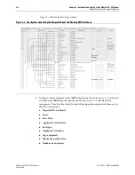
Page 26: ...f the APPS component shown in Figure 2 3 click on it and then select Edit from the right mouse menu Figure 2 4 illustrates this component Note that the values for the following parameters match those set in the DUT component Targeted Device Family Lanes Lane Rate Application Clock Rate Port type Application interface Tags supported Maximum payload size Number of Functions Figure 2 3 Qsys System Co...

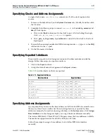
Page 27: ...arameters 5 To close the APPS component click the X in the upper right hand corner of the parameter editor 6 On the Qsys Generation tab specify the parameters listed in Table 2 15 Figure 2 4 Qsys Component Representing the Chaining DMA Design Table 2 7 Parameters to Specify on the Generation Tab in Qsys Part 1 of 2 Parameter Value Simulation Create simulation model Verilog This option creates a si...

Page 28: ... through steps to connect the chaining DMA component testbench f For further details about the parameter settings refer to Chapter 4 Parameter Settings Follow these steps to instantiate the Stratix V Hard IP for PCI Express and chaining DMA example design using the Qsys design flow 1 Create a directory for your project This example uses working_dir pcie_qsys 2 To start Qsys from the Quartus II sof...

Page 29: ...x V Hard IP for PCI Express to create a Gen1 8 Endpoint 1 Specify the System Settings listed in Table 2 8 2 Specify the BAR settings listed in Table 2 9 Table 2 8 System Settings Parameters Parameter Value Number of Lanes 8 Lane Rate Gen 1 2 5 Gbps Port type Native Endpoint PCI Express Base Specification version 2 1 Application interface Avalon ST 128 bit RX buffer credit allocation performance fo...

Page 30: ... Slot tab leave the Slot register turned off 11 Specify the Power Management settings listed in Table 2 13 12 On the PHY Characteristics tab select 53 for Full Swing Table 2 10 Device Identification Registers Register Name Value Vendor ID 0x00000000 Device ID 0x00000001 Revision ID 0x00000001 Class Code 0x00000000 Subsystem Vendor ID 0x00000000 Subsystem Device ID 0x00000001 Table 2 11 Device Para...

Page 31: ...he parameter values shown in Table 2 14 3 Click Finish 4 To rename the example design for Avalon Streaming Stratix V hard IP for PCI Express component right click on the component name select Rename and type APPSr Completing the Qsys System 1 To export the npor interface which is a power on reset pin for the FPGA click in the Export column and type pcie_rstn which is the name of the exported inter...

Page 32: ...tratix V Hard IP for PCI Express June 2012 Altera Corporation User Guide 1 Note that you must change the default name that Qsys provides for the exported interfaces Figure 2 5 illustrates the exported interfaces Figure 2 5 Qsys System Connecting the Endpoint Variant and Chaining DMA Testbench ...

Page 33: ... Name column right click on the rx_st interface and select and select Apps rx_st from the DUT rx_st Connections list 2 To connect the Avalon ST tx_st source interface of the APPS component to the tx_st sink interface of the DUT component repeat the technique explained in Step 1 Figure 2 6 illustrates this procedure For conduit interface types the APPS component interfaces connect to the DUT interf...

Page 34: ... APPS pld_clk_hip and select DUT pld_clk from the APPS pld_clk_hip Connections list c To connect the DUT coreclkout_hip interface to the APPS coreclkout_hip interface right click on DUT coreclkout_hip and select APPS coreclkout_hip from the DUT coreclkout_hip Connections list 5 To save your work on the File menu select Save and type pcie_de_gen1_x8_ast128 r in the Save dialog box 6 To remove the d...

Page 35: ... Flow Before compiling the complete example design in the Quartus II software you must add the example design files that you generated in Qsys to your Quartus II project Follow these steps to add the Quartus II IP File qip to the project 1 On the Project menu select Add Remove Files in Project 2 Click the browse button next the File name box and browse to the gen1_x8_example_design altera_pcie_sv_...

Page 36: ...The introduction does not display if you previously turned it off 5 On the Directory Name Top Level Entity page enter the following information a The working directory for your project This design example uses working_dir pcie_qsys b The name of the project Type the same name as your Qsys design pcie_de_gen1_x8_ast128 r 1 If the top level design entity and Qsys system names are identical the Quart...

Page 37: ...ay the EDA Tool Settings page 11 Click Next to display the Summary page 12 Check the Summary page to ensure that you have entered all the information correctly 13 Click Finish to create the Quartus II project 14 Add the Synopsys Design Constraint SDC shown inExample 2 2 to the top level design file for your Quartus II project 15 To compile your design using the Quartus II software on the Processin...

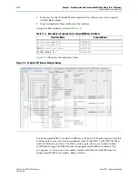
Page 38: ...generate the transactions needed to test your Application Layer Figure 2 7 Testbench for PCI Express PCB Avalon MM slave Reset Stratix V Hard IP for PCI Express Stratix V FPGA PCB Transaction Layer Data Link Layer PHY MAC Layer x8 PCIe Link Physical Layer Lane 7 Unused Unused Lane 6 Lane 5 TX PLL PHY IP Core for PCI Express Lane 2 Lane 3 Lane 4 Lane 1 Lane 0 TX PLL Transceiver Bank Transceiver Ban...

Page 39: ...o the Application Layer Gen2 1 Endpoint with a 64 bit Avalon MM interface to the Application Layer Gen2 4 Endpoint with a 128 bit Avalon MM interface to the Application Layer Gen2 8 Endpoint with a 128 bit Avalon MM interface to the Application Layer This example contains the following components Avalon MM Stratix V Hard IP for PCI Express 4 IP core On Chip memory DMA controller Transceiver reconf...

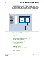
Page 40: ...ent is necessary for high performance transceiver designs This design example consists of the following steps 1 Creating a Quartus II Project 2 Running Qsys 3 Customizing the Avalon MM Stratix V Hard IP for PCI Express IP Core 4 Adding the Remaining Components to the Qsys System 5 Completing the Connections in Qsys 6 Specifying Clocks and Address Assignments 7 Specifying Exported Interfaces 8 Spec...

Page 41: ...es pcie_top You must specify the same name for both the project and the top level design entity 1 The Quartus II software specifies a top level design entity that has the same name as the project automatically Do not change this name 1 Click Yes if prompted to create a new directory 5 Click Next to display the Add Files page 6 If you have any non default libraries add them by following these steps...

Page 42: ...However this naming is not required for your own design If you want to choose a different name for the system file you must create a wrapper HDL file of the same name as the project s top level and instantiate the generated system 5 To add modules from the Component Library tab under Interface Protocols in the PCI folder click the Avalon MM Stratix V Hard IP for PCI Express component then click Ad...

Page 43: ...You can use the Auto Assign Base Addresses function on the System menu to define the address map For more information about the use of BARs to translate PCI Express addresses to Avalon MM addresses refer to PCI Express to Avalon MM Address Translation on page 5 15 Port type Native endpoint RX buffer credit allocation performance for received requests Low Reference clock frequency 100 MHz Use 62 5 ...

Page 44: ...ue Vendor ID 0x00000000 Device ID 0x00000001 Revision ID 0x00000001 Class Code 0x00000000 Subsystem Vendor ID 0x00000000 Subsystem Device ID 0x00000000 Table 3 5 PCI Express and PCI Capabilities Parameter Value Device Maximum payload size 128 Bytes Completion timeout range ABCD Implement completion timeout disable Turn on this option Error Reporting Advanced error reporting AER Turn off this optio...

Page 45: ... message area These values are computed based upon the values set for Maximum payload size and Desired performance for received requests Adding the Remaining Components to the Qsys System This section describes adding the DMA controller and on chip memory to your system 1 On the Component Library tab type the following text string in the search box DMA r Qsys filters the component library and show...

Page 46: ...he following text string in the search box On Chip r Qsys filters the component library and shows all components matching the text string you entered 6 Click On Chip Memory RAM or ROM and then click Add Specify the parameters listed in Table 3 9 Table 3 8 DMA Controller Parameters Parameter Value Width of the DMA length register 13 Enable burst transfers Turn on this option Maximum burst size Sele...

Page 47: ...sign it merges logical channels After compilation the design has two reconfiguration interfaces one for the TX PLL and one for the channels however the number of logical channels is still five 12 Click Finish 13 The Transceiver Reconfiguration Controller is added to your Qsys system Memory initialization Initialize memory content Turn off this option Enable non default initialization file Turn off...

Page 48: ...following procedure a Click the Rxm_BAR0 port then hover in the Connections column to display possible connections b Click the open dot at the intersection of the onchip_mem2_0 s1 port and the pci_express_compiler Rxm_BAR0 to create a connection 2 Repeat step 1 to make the connections listed in Table 3 11 Table 3 11 Qsys Connections Make Connection From To pcie_sv_hip_avmm_0 nreset_status Reset Ou...

Page 49: ...ign are connected to other modules outside the design Follow these steps to export an interface 1 Click in the Export column 2 Accept the default name that appears in the Export column Table 3 12 lists the interfaces that are exported Specifying Address Assignments Qsys requires that you resolve the base addresses of all Avalon MM slave interfaces in the Qsys system You can either use the auto ass...

Page 50: ... or 22 bits PCI Express requests that this BAR are able to access the Avalon addresses from 0x00200000 0x00200FFF BAR2 is sized to 32 KBytes or 15 bits The DMA control_port_slave is accessible at offsets 0x00004000 through 0x0000403F from the programmed BAR2 base address The pci_express CRA slave port is accessible at offsets 0x0000000 0x0003FFF from the programmed BAR2 base address Refer to Strat...

Page 51: ... directories that are generated in your Quartus II project directory 1 Note that Qsys automatically specifies subdirectories for Verilog Simulation and synthesis Simulating the Qsys System To simulate the example design you can include the simulation model in your own testbench Understanding Channel Placement Guidelines Stratix V transceivers are organized in banks of six channels The transceiver ...

Page 52: ...ter compilation expand the TimeQuest Timing Analyzer folder in the Compilation Report Note whether the timing constraints are achieved in the Compilation Report If your design does not initially meet the timing constraints you can find the optimal Fitter settings for your design by using the Design Space Explorer To use the Design Space Explorer click Launch Design Space Explorer on the tools menu...

Page 53: ...lication Layer Interface Avalon ST Avalon MM System Settings v v Base Address Register BAR and Expansion ROM Settings v v Base and Limit Registers for Root Ports v 1 Device Identification Registers v v PCI Express and PCI Capabilities Parameters v v Error Reporting v v Link Capabilities v v MSI and MSI X Capabilities v 2 Slot Capabilities v v Power Management v v Avalon Memory Mapped System Settin...

Page 54: ...tting displays in the message pane Refer to Chapter 12 Flow Control for more information about optimizing performance The Flow Control chapter explains how the RX credit allocation and the Maximum payload size that you choose affect the allocation of flow control credits You can set the Maximum payload size parameter on the Device tab The Message window of the GUI dynamically updates the number of...

Page 55: ...stems that include a 125 MHz clock source For more information about Gen3 operation refer to 4 3 8 Refclk Specifications for 8 0 GT s in the specification Use 62 5 MHz application clock On Off This is a special power saving mode available only for Gen1 1 and Gen2 1 variants Use deprecated RX Avalon ST data byte enable port rx_st_be On Off This parameter is not available for the Avalon MM Stratix V...

Page 56: ...For more information about channel placement refer to Serial Interface Signals on page 6 54 Note to Table 4 2 1 The Gen1 and Gen2 simulation models support pipe and serial simulation The Gen3 simulation model supports serial simulation only with equalization bypassed Table 4 2 System Settings for PCI Express Part 4 of 4 Parameter Value Description Table 4 3 BAR Registers Parameter Value Descriptio...
Page 57: ...O addressing Specifies the address widths for the Prefetchable Memory Base register and Prefetchable Memory Limit register Table 4 5 Device ID Registers Register Name Offset Address Range Default Value Description Vendor ID 16 bits 0x0000 Sets the read only value of the Vendor ID register This parameter can not be set to 0xFFFF per the PCI Express Specification Address 0x000 Device ID 16 bits 0x00...

Page 58: ...expected transaction sizes Address 0x084 Tags supported 32 64 32 Avalon ST 8 Avalon MM fixed Indicates the number of tags supported for non posted requests transmitted by the Application Layer This parameter sets the values in the Device Control register 0x088 of the PCI Express capability structure described in Table 7 8 on page 7 5 The Transaction Layer tracks all outstanding completions for non...

Page 59: ...ms to 250 ms Range C 250 ms to 4 s Range D 4 s to 64 s Bits are set to show timeout value ranges supported The function must implement a timeout value in the range 50 s to 50 ms The following values are used to specify the range None Completion timeout programming is not supported 0001 Range A 0010 Range B 0011 Ranges A and B 0110 Ranges B and C 0111 Ranges A B and C 1110 Ranges B C and D 1111 Ran...

Page 60: ...ble 4 7 1 Throughout the Stratix V Hard IP for PCI Express User Guide the terms word dword and qword have the same meaning that they have in the PCI Express Base Specification Revision 2 1 or 3 0 A word is 16 bits a dword is 32 bits and a qword is 64 bits Table 4 8 Link Capabilities 0x090 Parameter Value Description Link port number 0x01 Sets the read only value of the port number field in the Lin...
Page 61: ...le Offset 31 0 Points to the base of the MSI X Table The lower 3 bits of the table BAR indicator BIR are set to zero by software to form a 32 bit qword aligned offset 1 This field is read only MSI X Table BAR Indicator 2 0 Specifies which one of a function s BARs located beginning at 0x10 in Configuration Space is used to map the MSI X table into memory space This field is read only Legal range is...

Page 62: ...imit The following coefficients are defined 0 1 0x 1 0 1x 2 0 01x 3 0 001x The default value prior to hardware and firmware initialization is b 00 Writes to this register also cause the port to send the Set_Slot_Power_Limit Message Refer to Section 6 9 of the PCI Express Base Specification Revision 2 1 for more information Slot power limit 0 255 In combination with the Slot power scale value speci...

Page 63: ... enable Active State Power Management ASPM This setting is disabled for Root Ports The default value of this parameter is 64 ns This is the safest setting for most designs Endpoint L1 acceptable latency Maximum of 1 us Maximum of 2 us Maximum of 4 us Maximum of 8 us Maximum of 16 us Maximum of 32 us No limit This value indicates the acceptable latency that an Endpoint can withstand in the transiti...

Page 64: ...er resources than Completer Only This variant is targeted for systems that require simple read and write register accesses from a host CPU If you select this option the width of the data for RXM BAR masters is always 32 bits regardless of the Avalon MM width Control Register Access CRA Avalon slave port On Off Allows read and write access to bridge registers from the interconnect fabric using a sp...

Page 65: ...smission cyclical redundancy code CRC values and checks all CRCs during reception Manages the retry buffer and retry mechanism according to received ACK NAK Data Link Layer packets Initializes the flow control mechanism for DLLPs and routes flow control credits to and from the Transaction Layer Physical Layer The Physical Layer initializes the speed lane numbering and lane width of the PCI Express...

Page 66: ...t configuration Space Registers and a Type 1 Configuration TLP is used to access the Configuration Space Registers of downstream components typically Endpoints on the other side of the link The Hard IP includes dedicated clock domain crossing logic CDC between the PHYMAC and Data Link Layers This chapter provides an overview of the architecture of the Stratix V Hard IP for PCI Express It includes ...

Page 67: ...quests is partially supported Refer to the description of the rx_st_mask signal for further information about masking For more detailed information about the RX datapath refer to Avalon ST RX Interface on page 6 4 TX Datapath The TX datapath transports data from the Application Layer s Avalon ST interface to the Transaction Layer The Hard IP provides credit information to the Application Layer for...

Page 68: ...lates that the frequency of this clock be 100 MHz the Hard IP also accepts a 125 MHz reference clock as a convenience You can specify the frequency of your input reference clock using the parameter editor under the System Settings heading The PCI Express Base Specification also requires a system configuration time of 100 ms To meet this specification the Stratix V Hard IP for PCI Express includes ...

Page 69: ...er you cannot use the PIPE interface in actual hardware The Gen1 and Gen2 simulation models support pipe and serial simulation The Gen3 simulation model supports serial simulation only with equalization bypassed Transaction Layer The Transaction Layer is located between the Application Layer and the Data Link Layer It generates and receives Transaction Layer Packets Figure 5 3 illustrates the Tran...

Page 70: ... exist and acknowledges or postpones the request 4 The Transaction Layer forwards the TLP to the Data Link Layer Configuration Space The Configuration Space implements the following configuration registers and associated functions Header Type 0 Configuration Space for Endpoints Header Type 1 Configuration Space for Root Ports Figure 5 3 Architecture of the Transaction Layer Dedicated Receive Buffe...

Page 71: ...To Configuration Space Register Content on page 7 1 or Chapter 7 in the PCI Express Base Specification 2 1 for the complete content of these registers Data Link Layer The Data Link Layer DLL is located between the Transaction Layer and the Physical Layer It is responsible for maintaining packet integrity and for communication by DLL packet transmission at the PCI Express link level as opposed to c...

Page 72: ...lock generates transmit packets generating a sequence number and a 32 bit CRC LCRC The packets are also sent to the retry buffer for internal storage In retry mode the TLP generator receives the packets from the retry buffer and generates the CRC for the transmit packet Retry Buffer The retry buffer stores TLPs and retransmits all unacknowledged packets in the case of NAK DLLP reception For ACK DL...

Page 73: ...IP for PCI Express It is the layer closest to the link It encodes and transmits packets across a link and accepts and decodes received packets The Physical Layer connects to the link through a high speed SERDES interface running at 2 5 Gbps for Gen1 implementations at 2 5 or 5 0 Gbps for Gen2 implementations and at 2 5 5 0 or 8 0 Gbps for Gen 3 implementations The Physical Layer is responsible for...

Page 74: ...he PIPE interface specification The PHYMAC block is divided in four main sub blocks MAC Lane Both the RX and the TX path use this block On the RX side the block decodes the Physical Layer Packet and reports to the LTSSM the type and number of TS1 TS2 ordered sets received On the TX side the block multiplexes data from the DLL and the LTSTX sub block It also adds lane specific information including...

Page 75: ...ght word FIFO for each lane to store symbols Each symbol includes eight data bits one disparity bit and one control bit The FIFO discards the FTS COM and SKP symbols and replaces PAD and IDL with D0 0 data When all eight FIFOs contain data a read can occur When the multilane lane deskew block is first enabled each FIFO begins writing after the first COM is detected If all lanes have not detected a...

Page 76: ... requests It does not support bursting Figure 5 6 shows the block diagram of a full featured PCI Express Avalon MM bridge Figure 5 6 PCI Express Avalon MM Bridge Transaction Layer PCI Express Tx Controller PCI Express Rx Controller Data Link Layer Physical Layer PCI Express MegaCore Function Tx Slave Module Control Status Reg CSR Sync Avalon Clock Domain PCI Express Clock Domain Rx Master Module R...

Page 77: ...valon MM bridge converts the write requests to one or more PCI Express write packets with 32 or 64 bit addresses based on the address translation configuration the request address and the maximum payload size The Avalon MM write requests can start on any address in the range defined in the PCI Express address table parameters The bridge splits incoming burst writes that cross a 4 KByte boundary in...

Page 78: ... packets PCI Express to Avalon MM Downstream Write Requests When the PCI Express Avalon MM bridge receives PCI Express write requests it converts them to burst write requests before sending them to the interconnect fabric The bridge translates the PCI Express address to the Avalon MM address space based on the BAR hit information and on address translation table values configured during the IP cor...

Page 79: ...er the PCI Express PCI Capabilities heading in the parameter editor Refer to PCI Express and PCI Capabilities Parameters on page 4 6 PCI Express to Avalon MM Address Translation The PCI Express Avalon MM Bridge translates the system level physical addresses typically up to 64 bits to the 32 bit byte addresses used by the Application Layer You can specify up to six BARs for address translation when...

Page 80: ... of bits required to represent the address space supported by the upstream PCI Express device minus the number of bits required to represent the Size of address pages which are the LSB pass through bits N The Size of address pages N is applied to all entries in the translation table Each of the 512 possible entries corresponds to the base address of a PCI Express memory segment of a specific size ...

Page 81: ... perform simple read and write register accesses from a host CPU The completer only single dword endpoint is a hard IP implementation available for Qsys systems and includes an Avalon MM interface to the Application Layer The Avalon MM interface connection in this variation is 32 bits wide This endpoint is not pipelined at any time a single request can be outstanding The completer only single dwor...

Page 82: ...y reads and writes of a single dword It generates a completion with Completer Abort CA status for reads greater than four bytes and discards all write data without further action for write requests greater than four bytes The RX block passes header information to the Avalon MM master which generates the corresponding transaction to the Avalon MM interface The bridge accepts no additional requests ...

Page 83: ...SI Capability structure It is bit 16 of address 0x050 in the Configuration Space registers If the msi_enable bit is on an MSI request is sent to the Stratix V Hard IP for PCI Express when received otherwise INTX is signaled The interrupt handler block supports a single interrupt source so that software may assume the source You can disable interrupts by leaving the interrupt signal unconnected in ...

Page 84: ...5 20 Chapter 5 IP Core Architecture Completer Only Single Dword Endpoint Stratix V Hard IP for PCI Express June 2012 Altera Corporation User Guide ...

Page 85: ...saction Layer Packets TLPs into standard Avalon MM read and write commands typically used by master and slave interfaces to access memories and registers Consequently you do not need a detailed understanding of the PCI Express TLPs to use the Avalon MM variants Refer to Hard IP for PCI Express Features on page 1 3 to learn about the difference in the features available for the Avalon ST and Avalon...

Page 86: ...ext rxstatus 2 0 txblkst0 txsychd0 1 0 txdataskip0 rxblkst0 rxsynchd0 1 0 rxdataskip0 simu_mode_pipe ltssmstate 4 0 rate 1 0 pclk_in tx_margin 2 0 txswing testin_zero 8 bit PIPE PIPE Simulation Only for Gen1 and Gen2 Gen3 Provides Serial Simulation test_in 31 0 lane_act 3 0 tl_cfg_add 3 0 tl_cfg_ctl 31 0 tl_cfg_sts 52 0 hpg_ctrler 4 0 lmi_dout 31 0 lmi_rden lmi_wren lmi_ack lmi_addr 11 0 lmi_din 3...

Page 87: ...on Side Band Signals on page 6 33 Configuration space Transaction Layer Configuration Space Signals on page 6 34 Parity Error Parity Signals on page 6 41 LMI LMI Signals on page 6 42 Hard IP reconfiguration block Hard IP Reconfiguration Interface on page 6 44 Power management Power Management Signals on page 6 46 Physical Transceiver control Transceiver Reconfiguration on page 6 53 Serial Serial I...

Page 88: ... is qword aligned The mapping of message TLPs is the same as the mapping of TLPs with 4 dword headers When using a 64 bit Avalon ST bus the width of rx_st_data is 64 When using a 128 bit Avalon ST bus the width of rx_st_data is 128 When using a 256 bit Avalon ST bus the width of rx_st_data is 256 bits rx_st_sop 1 2 O start of packet Indicates that this is the first cycle of the TLP when rx_st_vali...

Page 89: ... bit 1 applies to the eop occurring in rx_st_data 255 128 bit 0 applies to the eop occurring in rx_st_data 127 0 When the TLP ends in the lower 128bits the following equations apply rx_st_eop 0 1 rx_st_empty 0 0 rx_st_data 127 0 contains valid data rx_st_eop 0 1 rx_st_empty 0 1 rx_st_data 63 0 contains valid data rx_st_data 127 64 is empty When TLP ends in the upper 128bits the following equations...

Page 90: ...be asserted at any time The total number of non posted requests that can be transferred to the Application Layer after rx_st_mask is asserted is not more than 10 rx_st_bardec1 rx_st_bardec2 8 O component specific The decoded BAR bits for the TLP Valid for MRd MWr IOWR and IORD TLPs ignored for the completion or message TLPs rx_st_bardec1 is valid on the first cycle of rx_st_data for TLPs that begi...

Page 91: ...ligned to qword boundary for completion with data TLPs that are for configuration read or I O read requests rx_st_be deprecated 8 16 32 O component specific Byte enables corresponding to the rx_st_data The byte enable signals only apply to PCI Express TLP payload fields When using 64 bit Avalon ST bus the width of rx_st_be is 8 bits When using 128 bit Avalon ST bus the width of rx_st_be is 16 bits...

Page 92: ...d and ends with 0x4 causing the first data to correspond to rx_st_data 63 32 Figure 6 2 Qword Alignment 0x0 0x8 0x10 0x18 Header Addr 0x4 64 bits PCB Memory Valid Data Valid Data Table 6 4 Mapping Avalon ST Packets to PCI Express TLPs Packet TLP Header0 pcie_hdr_byte0 pcie_hdr _byte1 pcie_hdr _byte2 pcie_hdr _byte3 Header1 pcie_hdr _byte4 pcie_hdr _byte5 pcie_hdr byte6 pcie_hdr _byte7 Header2 pcie...

Page 93: ... four dword header with qword aligned addresses with a 64 bit bus Figure 6 3 64 Bit Avalon ST rx_st_data n Cycle Definition for 3 Dword Header TLPs with Non Qword Aligned Address pld_clk rx_st_data 63 32 rx_st_data 31 0 rx_st_sop rx_st_eop rx_st_be 7 4 rx_st_be 3 0 Header1 Data0 Data2 Header0 Header2 Data1 F F F Figure 6 4 64 Bit Avalon ST rx_st_data n Cycle Definition for 3 Dword Header TLPs with...

Page 94: ...deasserting rx_st_ready The rx_st_valid signal deasserts within three cycles after rx_st_ready is deasserted In this example rx_st_valid is deasserted in the next cycle rx_st_data is held until the Application Layer is able to accept it Figure 6 6 64 Bit Avalon ST rx_st_data n Cycle Definitions for 4 Dword Header TLPs with Non Qword Addresses 1 Note to Figure 6 6 1 rx_st_be 7 4 corresponds to rx_s...

Page 95: ...eader and qword aligned addresses The assertion of rx_st_empty in a rx_st_eop cycle indicates valid data on the lower 64 bits of rx_st_data Figure 6 8 64 Bit Avalon ST Interface Back to Back Transmission pld_clk rx_st_data 63 0 rx_st_sop rx_st_eop rx_st_ready rx_st_valid C C C C CCCC0089002 C C C C C C C C C C C C C C C C C C C C C C C C C C C C Figure 6 9 128 Bit Avalon ST rx_st_data n Cycle Defi...

Page 96: ...ader with non qword aligned addresses In this example rx_st_empty is low because the data is valid for all 128 bits in the rx_st_eop cycle Figure 6 10 128 Bit Avalon ST rx_st_data n Cycle Definition for 3 Dword Header TLPs with non Qword Aligned Addresses rx_st_valid rx_st_data 127 96 rx_st_data 95 64 rx_st_data 63 32 rx_st_data 31 0 rx_st_sop rx_st_eop rx_st_empty Data0 Data 4 Header 2 Data 3 Hea...

Page 97: ...n three cycles after rx_st_ready is deasserted In this example rx_st_valid is deasserted in the next cycle rx_st_data is held until the Application Layer is able to accept it Figure 6 12 128 Bit Avalon ST rx_st_data Cycle Definition for 4 Dword Header TLPs with Qword Aligned Addresses pld_clk rx_st_valid rx_st_data 127 96 rx_st_data 95 64 rx_st_data 63 32 rx_st_data 31 0 rx_st_sop rx_st_eop rx_st_...

Page 98: ... Appendix A Transaction Layer Packet TLP Header Formats Single Packet Per Cycle In single packer per cycle mode all received TLPs start at the lower 128 bit boundary on a 256 bit Avalon ST interface Turn on Enable Multiple Packets per Cycle on the System Settings tab of the parameter editor to change multiple packets per cycle Figure 6 14 128 Bit Avalon ST Interface Back to Back Transmission pld_c...

Page 99: ... shows the location of headers and data for the 256 bit Avalon ST packets This layout of data applies to both the TX and RX buses Figure 6 17 illustrates two single cycle 256 bit packets The first packet has two empty qword rx_st_data 191 0 is valid The second packet has two empty dwords rx_st_data 127 0 is valid Figure 6 16 Location of Headers and Data for Avalon ST 256 Bit Interface D3 255 0 255...

Page 100: ...its of the Avalon ST interface because a new TLP can start in the lower 128 bit Avalon ST interface This mode adds complexity to the Application Layer user decode logic However it could result in higher throughput Figure 6 18 illustrates this mode for a 256 bit Avalon ST RX interface In this figure rx_st_eop 0 and rx_st_sop 1 are asserted in the same cycle Figure 6 18 256 Bit Avalon ST RX Interfac...

Page 101: ...dicates first cycle of a TLP when asserted together with tx_st_valid When using a 256 bit Avalon ST bus with Multiple packets per cycle bit 0 indicates that a TLP begins in tx_st_data 127 0 bit 1 indicates that a TLP begins in tx_st_data 255 128 tx_st_eop 1 2 I end of packet Indicates last cycle of a TLP when asserted together with tx_st_valid When using a 256 bit Avalon ST bus with Multiple packe...

Page 102: ...hether the upper qword contains data For 256 bit data both bits are used to indicate the number of upper words that contain data resulting in the following encodings for the 128 and 256 bit interfaces 128 Bit interface tx_st_empty 0 tx_st_data 127 0 contains valid data tx_st_empty 1 tx_st_data 63 0 contains valid data 256 bit interface tx_st_empty 0 tx_st_data 255 0 contains valid data tx_st_empty...

Page 103: ... 15 8 and so on Component Specific Signals tx_cred_datafccp 12 O component specific Data credit limit for the received FC completions Each credit is 16 bytes tx_cred_datafcnp 12 O component specific Data credit limit for the non posted requests Each credit is 16 bytes tx_cred_datafcp 12 O component specific Data credit limit for the FC posted writes Each credit is 16 bytes tx_cred_fchipcons 6 O co...

Page 104: ...ic Header limit for the non posted requests Each credit is 20 bytes tx_cred_hdrfcp 8 O component specific Header credit limit for the FC posted writes Each credit is 20 bytes ko_cpl_spc_header 8 O component specific The Application Layer can use this signal to build circuitry to prevent RX buffer overflow for completion headers Endpoints must advertise infinite space for completion headers however...

Page 105: ... pcie_hdr_byte4 pcie_hdr _byte5 header pcie_hdr byte6 pcie_hdr _byte7 3 Header2 pcie_hdr _byte8 pcie_hdr _byte9 pcie_hdr _byte10 pcie_hdr _byte11 4 Data0 pcie_data_byte3 pcie_data_byte2 pcie_data_byte1 pcie_data_byte0 5 Data1 pcie_data_byte7 pcie_data_byte6 pcie_data_byte5 pcie_data_byte4 6 Data2 pcie_data_byte11 pcie_data_byte10 pcie_data_byte9 pcie_data_byte8 pld_clk tx_st_data 63 32 tx_st_data ...

Page 106: ... after tx_st_ready is asserted Figure 6 23 illustrates back to back transmission of 64 bit packets with no idle cycles between the assertion of tx_st_eop and tx_st_sop Figure 6 21 64 Bit Avalon ST tx_st_data Cycle Definition for TLP 4 Dword Header with Non Qword Aligned Address pld_clk tx_st_data 63 32 tx_st_data 31 0 tx_st_sop tx_st_eop Header 1 Header3 Data0 Data2 Header 0 Header2 Data1 Figure 6...

Page 107: ...ress TLPs for a 3 dword header with non qword aligned addresses It also shows tx_st_err assertion Figure 6 24 128 Bit Avalon ST tx_st_data Cycle Definition for 3 Dword Header TLP with Qword Aligned Address Data3 Header2 Data 2 Header1 Data1 Data n Header0 Data0 Data n 1 pld_clk tx_st_valid tx_st_data 127 96 tx_st_data 95 64 tx_st_data 63 32 tx_st_data 31 0 tx_st_sop tx_st_eop tx_st_empty Figure 6 ...

Page 108: ...e the data ends in the upper 64 bits of tx_st_data Figure 6 26 128 Bit Avalon ST tx_st_data Cycle Definition for 4 Dword Header TLP with Qword Aligned Address pld_clk tx_st_data 127 96 tx_st_data 95 64 tx_st_data 63 32 tx_st_data 31 0 tx_st_sop tx_st_eop tx_st_empty Header 3 Data 3 Header 2 Data 2 Header 1 Data 1 Header 0 Data 0 Data 4 Figure 6 27 128 Bit Avalon ST tx_st_data Cycle Definition for ...

Page 109: ...easserts tx_st_valid after two cycles and holds tx_st_data until two cycles after tx_st_ready is reasserted Data Alignment and Timing for the 256 Bit Avalon ST TX Interface Refer to Figure 6 16 on page 6 15 layout of headers and data for the 256 bit Avalon ST packets with qword aligned and qword unaligned addresses Figure 6 28 128 Bit Back to Back Transmission on the Avalon ST TX Interface pld_clk...

Page 110: ... always start in the lower 128 bits of the Avalon ST interface Although this mode simplifies the Application Layer logic failure to use the full 256 bit Avalon ST may slightly reduce the throughput of a design Figure 6 30 illustrates the layout of header and data for a three dword header on a 256 bit bus with aligned and unaligned data Figure 6 30 256 Bit Avalon ST tx_st_data Cycle Definition for ...

Page 111: ...should be no ECRC appended to the TLP and the TD bit in the TLP header should be set to 0 These packets are processed internally by the Hard IP block and are not transmitted on the PCI Express link ECRC Forwarding On the Avalon ST interface the ECRC field follows the same alignment rules as payload data For packets with payload the ECRC is appended to the data as an extra dword of payload For pack...

Page 112: ...uency clock used by the Data Link and Transaction Layers To meet PCI Express link bandwidth constraints this clock has minimum frequency requirements as listed in Table 8 2 on page 8 6 Note to Table 6 6 1 Figure 8 5 on page 8 5 illustrates these clock signals Table 6 7 Reset and Link Training Signals Part 1 of 3 Signal I O Description npor I Active low reset signal It is the OR of pin_perst and lo...

Page 113: ...ot 3 3V if the following 2 conditions are met The input signal meets the VIH and VIL specification for LVTTL The input signal meets the overshoot specification for 100 C operation as specified by the Maximum Allowed Overshoot and Undershoot Voltage section in volume 3 of the Stratix V Device Handbook Refer to Figure 6 32 on page 6 31 for a timing diagram illustrating the use of this signal serdes_...

Page 114: ...es currentspeed 1 0 O Indicates the current speed of the PCIe link The following encodings are defined 2b 00 Undefined 2b 01 Gen1 2b 10 Gen2 2b 11 Gen3 ltssmstate 4 0 O LTSSM state The LTSSM state machine encoding defines the following states 00000 Detect Quiet 00001 Detect Active 00010 Polling Active 00011 Polling Compliance 00100 Polling Configuration 00101 Polling Speed 00110 config Linkwidthst...

Page 115: ... characterization npor IO_POF_Load PCIe_LinkTraining_Enumeration dl_ltssm 4 0 detect detect active polling active L0 100 ms Table 6 8 ECC Error Signals for Hard IP Implementation 1 Signal I O Description derr_cor_ext_rcv O Indicates a corrected error in the RX buffer This signal is for debug only It is not valid until the RX buffer is filled with data This is a pulse not a level signal Internally ...

Page 116: ...ol register apply Refer to Table 6 17 on page 6 40 for more information app_int_sts I Controls legacy interrupts Assertion of app_int_sts causes an Assert_INTA message TLP to be generated and sent upstream Deassertion of app_int_sts causes a Deassert_INTA message TLP to be generated and sent upstream app_int_ack O This signal is the acknowledge for app_int_sts This signal is asserted for at least ...

Page 117: ...ation Space When an error occurs the appropriate signal is asserted for one cycle cpl_err 0 Completion timeout error with recovery This signal should be asserted when a master like interface has performed a non posted request that never receives a corresponding completion transaction after the 50 ms timeout period when the error is correctable The Hard IP automatically generates an advisory error ...

Page 118: ...action Layer Errors on page 13 3 cpl_err 6 Log header If header logging is required this bit must be set in the every cycle in which any of cpl_err 2 cpl_err 3 cpl_err 4 or cpl_err 5 is set The Application Layer presents the header to the Hard IP by writing the following values to the following 4 registers using LMI before asserting cpl_err 6 lmi_addr 12 h81C lmi_din err_desc_func0 127 96 lmi_addr...

Page 119: ...This signal should be asserted when the power controller detects a power fault for this slot If this slot has no power controller this bit should be hardwired to 0 and the Power Controller Present bit bit 1 in the Slot capability register parameter is set to 0 I 4 Power controller status This signal is used to set the command completed bit of the Slot Status register Power controller status is equ...

Page 120: ...t Bit 12 received target abort Bit 11 signalled target abort 24 Secondary Status Register 8 Master data parity error 23 6 Root Status Register 17 0 Records the following PME status information Bit 17 PME pending Bit 16 PME status Bits 15 0 PME request ID 15 0 5 1 Secondary Status Register 15 11 Records the following 5 secondary command status errors Bit 15 detected parity error Bit 14 received sys...

Page 121: ...trl 7 0 4 cfg_sec_ctrl 15 0 cfg_secbus 7 0 cfg_subbus 7 0 5 cfg_msi_addr 11 0 cfg_io_bas 19 0 6 cfg_msi_addr 43 32 cfg_io_lim 19 0 7 8h 00 cfg_np_bas 11 0 cfg_np_lim 11 0 8 cfg_pr_bas 31 0 9 cfg_msi_addr 31 12 cfg_pr_bas 43 32 A cfg_pr_lim 31 0 B cfg_msi_addr 63 44 cfg_pr_lim 43 32 C cfg_pmcsr 31 0 D cfg_msixcsr 15 0 cfg_msicsr 15 0 E 6 h00 tx_ecrcgen 25 3 rx_ecrccheck 24 cfg_tcvcmap 23 0 F cfg_ms...

Page 122: ..._ctrl2 15 0 the primary Link Status register contents is available on tl_cfg_sts 46 31 For Gen1 variants the link bandwidth notification bit is always set to 0 For Gen2 variants this bit is set to 1 Table 7 8 on page 7 5 0x0B0 Gen2 only cfg_prm_cmd 16 O Base Primary Control and Status register for the PCI Configuration Space Table 7 2 on page 7 2 0x004 Type 0 Table 7 3 on page 7 2 0x004 Type 1 cfg...

Page 123: ...pper 44 bits of the prefetchable limit registers of the Type1 Configuration Space Available in Root Port mode Table 7 3 on page 7 2 0x024 and Table 4 3 on page 4 4 prefetchable memory cfg_pmcsr 32 O cfg_pmcsr 31 16 is Power Management Control and cfg_pmcsr 15 0 is the Power Management Status register Table 7 6 on page 7 4 0x07C cfg_msixcsr 16 O MSI X message control Table 7 5 on page 7 3 0x068 cfg...

Page 124: ... enable multiple message capable MSI enable Table 6 17 Configuration MSI Control Status Register Field Descriptions Part 1 of 2 Bit s Field Description 15 9 reserved 8 mask capability Per vector masking capable This bit is hardwired to 0 because the function does not support the optional MSI per vector masking using the Mask_Bits and Pending_Bits registers defined in the PCI Local Bus Specificatio...

Page 125: ...to 32 parity bits are propagated to the Application Layer along with the RX Avalon ST data The RX datapath also propagates up to 32 parity bits to the Transaction Layer for Configuration TLPs On the TX datapath parity generated in the Application Layer is checked in Transaction Layer and the Data Link Layer 3 1 multiple message capable Multiple message capable This field is read by system software...

Page 126: ...egisters For more information refer to Uncorrectable Internal Error Status Register on page 7 9 rx_par_err O When asserted for a single cycle indicates that a parity error was detected in a TLP at the input of the RX buffer This error is logged as an uncorrectable internal error in the VSEC registers For more information refer to Uncorrectable Internal Error Status Register on page 7 9 If this err...

Page 127: ...tion TLP accesses are no longer pending An acknowledge signal is sent back to the Application Layer when the execution is complete All LMI reads are also held and executed when no configuration TLP requests are pending The LMI interface supports two operations local read and local write The timing for these operations complies with the Avalon MM protocol described in the Avalon Interface Specifica...

Page 128: ...dress and 16 bit data You can use this bus dynamically modify the value of configuration registers that are read only at run time Tp ensure proper system operation Altera recommends that you reset or repeat device enumeration of the PCI Express link after changing the value of read only configuration registers of the Hard IP For a description of the registers available via this interface refer to ...

Page 129: ...ad signal This interface is not pipelined You must wait for the return of the hip_reconfig_readdata 15 0 from the current read before starting another read operation hip_reconfig_readdata 15 0 O 16 bit read data hip_reconfig_readdata 15 0 is valid on the third cycle after the assertion of hip_reconfig_read hip_reconfig_write I Write signal hip_reconfig_writedata 15 0 I 16 bit write model hip_recon...

Page 130: ...from the low power state to send the message This signal is positive edge sensitive pm_data 9 0 I Power Management Data This bus indicates power consumption of the component This bus can only be implemented if all three bits of AUX_power part of the Power Management Capabilities structure are set to 0 This bus includes the following bits pm_data 9 2 Data Register This register maintains a value as...

Page 131: ...cates that the function would normally assert the PME message independently of the state of the PME_en bit 14 13 data_scale This field indicates the scaling factor when interpreting the value retrieved from the data register This field is read only 12 9 data_select This field indicates which data should be reported through the data register and the data_scale field 8 PME_EN 1 indicates that the fu...

Page 132: ...readdata 63 0 txs_waitrequest 32 Bit Avalon MM CRA Slave Port Optional Not available for Completer Only Single Dword 64 Bit Avalon MM TX Slave Port Not used for Completer Only Avalon MM Stratix V Hard IP for PCI Express Test Interface test_in 31 0 mode rxm_bar0_write_ n rxm_bar0_address_ n 31 0 rxm_bar0_writedata_ n 63 0 or 31 0 rxm_bar0_byteenable_ n 7 0 rxm_bar0_burstcount_ n 6 0 rxm_bar0_waitre...

Page 133: ... Slave Signals on page 6 49 Avalon MM RX Master v v RX Avalon MM Master Signals on page 6 50 Avalon MM TX Slave v 64 Bit Bursting TX Avalon MM Slave Signals on page 6 51 Clock v v Clock Signals on page 6 28 Reset and Status v v Reset Signals and Status Signals on page 6 28 Physical and Test Transceiver Control v v Transceiver Reconfiguration on page 6 53 Serial v v Serial Interface Signals on page...

Page 134: ...ta being written to slave w 64 for the full featured IP core w 32 for the completer only IP core rxm_bar0_byteenable_ n w 1 0 O Byte enable for write data rxm_bar0_burstcount_ n 6 0 O The burst count measured in qwords of the RX write or read request The width indicates the maximum data that can be requested The maximum data in a burst is 512 bytes rxm_bar0_waitrequest_ n I Asserted by the externa...

Page 135: ...nterconnect fabric are translated into PCI Express request packets Incoming requests can be up to 512 bytes For better performance Altera recommends using smaller read request size a maximum of 512 bytes Figure 6 40 Simultaneous DMA Read DMA Write and Target Access RxmRead_o RxmReadDataValid_i RxmReadData_i 63 0 RxmResetRequest_o RxmAddress_o 31 0 RxmWaitRequest_i RxmWrite_o RxmBurstCount_o 9 0 Rx...

Page 136: ...his behavior is most easily implemented with a store and forward buffer in the Avalon MM master txs_writedata 63 0 I Write data sent by the external Avalon MM master to the TX slave port txs_burstcount 6 0 I Asserted by the system interconnect fabric indicating the amount of data requested The count unit is the amount of data that is transferred in a single cycle that is the width of the bus The b...

Page 137: ...e I O Description reconfig_from_xcvr n 46 1 0 reconfig_to_xcvr n 70 1 0 O These are the parallel transceiver dynamic reconfiguration buses Dynamic reconfiguration is required to compensate for variations due to process voltage and temperature PVT Among the analog settings that you can reconfigure are VOD pre emphasis and equalization You can use the Altera Transceiver Reconfiguration Controller to...

Page 138: ...the CMU PLL Table 6 30 1 Bit Interface Signals Signal I O Description tx_out 7 0 1 O Transmit input These signals are the serial outputs of lanes 7 0 rx_in 7 0 1 I Receive input These signals are the serial inputs of lanes 7 0 Note to Table 6 30 1 The 1 IP core only has lane 0 The 4 IP core only has lanes 3 0 Figure 6 41 Channel Placement Gen1 and Gen2 x1 and x4 Variants Gen1 and Gen 2 x1 Transcei...

Page 139: ...ng CMU PLL Channel 0 Data Channel 1 Data Channel 2 Data Channel 4 CMU PLL Channel 5 Data Channel 3 Data Transceiver Bank 1 Gen1 and Gen2 x8 Transceiver Bank 0 Channel 6 Data Available for Other Protocols Channel 7 Data Channel 8 Data Channel 10 Channel 11 PCS Clock and Control Signals Channel 9 CCD CCD Central Clock Divider PCI Express Lane 0 PCI Express Lane 1 PCI Express Lane 2 PCI Express Lane ...

Page 140: ... Placement Gen3 8 Variants Using ATX PLL Channel 0 Data Channel 1 Data Channel 2 Data Channel 4 CMU PLL Channel 5 Data Channel 3 Data Transceiver Bank 1 Gen3 Transceiver Bank 0 Channel 6 Data Available for Other Protocols Channel 7 Data Channel 8 Data Channel 10 Channel 11 Channel 9 CCD CCD Central Clock Divider PCI Express Lane 0 PCI Express Lane 1 PCI Express Lane 2 PCI Express Lane 3 PCI Expres...

Page 141: ...igure 6 44 illustrates the channel placement for Gen1 and Gen2 1 and 4 variants when you select the ATX PLL Figure 6 44 Channel Placement Gen1 and Gen2 Using ATX PLL Gen1 and Gen 2 x1 Transceiver Bank LCD ATX PLL0 LCD Local Clock Divider Channel 0 Data Channel 1 CMU PLL Channel 2 Data Channel 4 Channel 5 PCI Express Lane 0 Channel 3 Other Protocols CCD Central Clock Divider Other Protocols Transce...

Page 142: ...nnel 1 Data Channel 2 Data Channel 4 CMU PLL Channel 5 Data Channel 3 Data Transceiver Bank 1 Gen1 and Gen2 x8 Transceiver Bank 0 Available for Other Protocols CCD CCD Central Clock Divider PCI Express Lane 0 PCI Express Lane 1 PCI Express Lane 2 PCI Express Lane 3 Unavailable Channel PCI Express Lane 4 PCI Express Lane 5 PCI Express Lane 6 PCI Express Lane 7 ATX PLL1 Channel 6 Data Channel 7 Data...

Page 143: ...n includes the serial interface to the internal transceivers However it is not possible to use the Hard IP PIPE interface in hardware including probing these signals using SignalTap II Embedded Logic Analyzer 1 The Gen3 simulation model supports serial only simulation with equalization bypassed Figure 6 46 Channel Placement Gen3 1 and 4 Transceiver Bank Gen3 x1 Transceiver Bank LCD LCD Local Clock...

Page 144: ...specified state P0 P0s P1 or P2 tx_deemph0 O Transmit de emphasis selection The Stratix V Hard IP for PCI Express sets the value for this signal based on the indication received from the other end of the link during the Training Sequences TS You do not need to change this value rxdata0 7 0 1 2 I Receive data n 2 symbols on lane n This bus receives data on lane n rxdatak0 1 2 I Receive data n This ...

Page 145: ...s are defined 2 b01 Ordered Set Block 2 b10 Data Block rxdataskip0 I For Gen3 operation Allows the PCS to instruct the RX interface to ignore the RX data interface for one clock cycle The following encodings are defined 1 b0 RX data is invalid 1 b1 RX data is valid ltssmstate0 4 0 LTSSM state The LTSSM state machine encoding defines the following states 5 b00000 Detect Quiet 5 b 00001 Detect Activ...

Page 146: ... 5 b10101 LOs 5 b11001 L2 transmit Wake 5 b11010 Speed Recovery 5 b11011 Recovery Equalization Phase 0 5 b11100 Recovery Equalization Phase 1 5 b11101 Recovery Equalization Phase 2 5 b11110 recovery Equalization Phase 3 rate 1 0 O The 2 bit encodings have the following meanings 2 b00 Gen1 rate 2 5 Gbps 2 b01 Gen2 rate 5 0 Gbps 2 b1X Gen3 rate 8 0 Gbps pclk_in I This clock is used for PIPE simulati...

Page 147: ...01000 5 Compliance test mode Disable force compliance mode When set prevents the LTSSM from entering compliance mode Toggling this bit controls the entry and exit from the compliance state enabling the transmission of Gen1 Gen2 and Gen3 compliance patterns 31 6 Reserved Must be set to 26 h2 simu_mode_pipe O When set to 1 the PIPE interface is in simulation mode lane_act 3 0 Lane Active Mode This s...

Page 148: ...6 64 Chapter 6 IP Core Interfaces Test Signals Stratix V Hard IP for PCI Express June 2012 Altera Corporation User Guide ...

Page 149: ... 0 Compatible Configuration Space Header Refer to Table 7 2 for details 0x000 0x03C PCI Type 1 Compatible Configuration Space Header Refer to Table 7 3 for details 0x040 0x04C Reserved 0x050 0x05C MSI Capability Structure Refer to Table 7 4 for details 0x060 0x064 Reserved 0x068 0x070 MSI X Capability Structure Refer to Table 7 5 for details 0x070 0x074 Reserved 0x078 0x07C Power Management Capabi...

Page 150: ...ddress Register BAR and Expansion ROM Settings 0x014 Base Address Register BAR and Expansion ROM Settings 0x018 Base Address Register BAR and Expansion ROM Settings 0x01C Base Address Register BAR and Expansion ROM Settings 0x020 Base Address Register BAR and Expansion ROM Settings 0x024 Base Address Register BAR and Expansion ROM Settings 0x028 Reserved 0x02C Subsystem Device ID Subsystem vendor ...

Page 151: ...etween the Configuration Space registers and the PCI Express Base Specification 2 0 Table 7 3 PCI Type 1 Configuration Space Header Root Ports Rev3 0 Spec Type 1 Configuration Space Header Part 2 of 2 Byte Offset 31 24 23 16 15 8 7 0 Table 7 4 MSI Capability Structure Rev3 0 Spec MSI Capability Structures Byte Offset 1 31 24 23 16 15 8 7 0 0x050 Message Control Configuration MSI Control Status Reg...

Page 152: ...Data PM Control Status Bridge Extensions Power Management Status Control Note to Table 7 6 1 Refer to Table 7 36 on page 7 18 for a comprehensive list of correspondences between the Configuration Space registers and the PCI Express Base Specification 2 0 Table 7 7 PCI Express AER Capability Structure Rev3 0 Spec AER Capability Byte Offset 31 24 23 16 15 8 7 0 0x800 PCI Express Enhanced Capability ...

Page 153: ...lot Capabilities 0x098 Slot Status Slot Control 0x09C Root Capabilities Root Control 0x0A0 Root Status 0x0A4 Device Capabilities 2 0x0A8 Device Status 2 Device Control 2 0x0AC Link Capabilities 2 0x0B0 Link Status 2 Link Control 2 0x0B4 Slot Capabilities 2 0x0B8 Slot Status 2 Slot Control 2 Note to Table 7 8 1 Registers not applicable to a device are reserved 2 Refer to Table 7 36 on page 7 18 for...

Page 154: ...e Offset Register Name 31 20 19 16 15 8 7 0 Table 7 10 Altera Defined VSEC Capability Header Bits Register Description Value Access 15 0 PCI Express Extended Capability ID PCIe specification defined value for VSEC Capability ID 0x000B RO 19 16 Version PCIe specification defined value for VSEC version 0x1 RO 31 20 Next Capability Offset Starting address of the next Capability Structure implemented ...

Page 155: ...O Table 7 15 CvP Status Bits Register Description Reset Value Access 15 10 Reserved 0x00 RO 9 PLD_CORE_READY From FPGA fabric This status bit is provided for debug Variable RO 8 PLD_CLK_IN_USE From clock switch module to fabric This status bit is provided for debug Variable RO 7 CVP_CONFIG_DONE Indicates that the FPGA control block has completed the device configuration via CvP and there were no e...

Page 156: ...3F corresponds to 1 to 63 clock cycles The upper bits are not used but are included in this field because they belong to the same byte enable 0x00 RW 7 4 Reserved 0x0 RO 2 CVP_FULLCONFIG Request that the FPGA control block reconfigure the entire FPGA including the Stratix V Hard IP for PCI Express bring the PCIe link down 1 b0 RW 1 HIP_CLK_SEL Selects between PMA and fabric clock when USER_MODE 1 ...

Page 157: ...1 b0 RW 0 CVP_CONFIG When asserted instructs that the FPGA control block begin a transfer via CvP 1 b0 RW Table 7 19 Uncorrectable Internal Error Status Register Bits Register Description Access 31 12 Reserved RO 11 When set indicates an RX buffer overflow condition in a posted request or Completion RW1CS 10 Reserved RO 9 When set indicates a parity error was detected on the Configuration Space to...

Page 158: ...ion Reset Value Access 31 12 Reserved 1b 0 RO 11 Mask for RX buffer posted and completion overflow error 1b 1 RWS 10 Reserved 1b 0 RO 9 Mask for parity error detected on Configuration Space to TX bus interface 1b 1 RWS 8 Mask for parity error detected on the TX to Configuration Space bus interface 1b 1 RWS 7 Mask for parity error detected at TX Transaction Layer error 1b 1 RWS 6 Reserved 1b 0 RO 5...

Page 159: ...V Hard IP for PCI Express are routed through the interconnect fabric hardware does not enforce restrictions to limit individual processor access to specific regions However the regions are designed to enable straight forward enforcement by processor software Figure 7 1 illustrates accesses to the Avalon MM control and status registers from the Host CPU and PCI Express link Table 7 22 Correctable I...

Page 160: ... bridge mailbox registers and read access to Avalon MM to PCI Express mailbox registers 0x1000 0x1FFF Avalon MM to PCI Express address translation tables Depending on the system design these may be accessed by PCI Express processors Avalon MM processors or both 0x2000 0x2FFF Reserved 0x3000 0x3FFF Registers typically intended for access by Avalon MM processors only These include Avalon MM interrup...

Page 161: ...T5 RW1C 1 when the A2P_MAILBOX5 is written to 20 A2P_MAILBOX_INT4 RW1C 1 when the A2P_MAILBOX4 is written to 19 A2P_MAILBOX_INT3 RW1C 1 when the A2P_MAILBOX3 is written to 18 A2P_MAILBOX_INT2 RW1C 1 when the A2P_MAILBOX2 is written to 17 A2P_MAILBOX_INT1 RW1C 1 when the A2P_MAILBOX1 is written to 16 A2P_MAILBOX_INT0 RW1C 1 when the A2P_MAILBOX0 is written to 15 0 AVL_IRQ_ASSERTED 15 0 RO Current v...

Page 162: ..._IRQ_VECTOR RO Stores the interrupt vector of the system interconnect fabric The host software should read this register after being interrupted and determine the servicing priority Table 7 28 PCI Express to Avalon MM Mailbox Registers 0x0800 0x081F Address Name Access Description 0x0800 P2A_MAILBOX0 RW PCI Express to Avalon MM Mailbox 0 0x0804 P2A_MAILBOX1 RW PCI Express to Avalon MM Mailbox 1 0x...

Page 163: ...ddress map entry 0 0x1004 31 0 A2P_ADDR_MAP_HI0 RW Upper bits of Avalon MM to PCI Express address map entry 0 0x1008 1 0 A2P_ADDR_SPACE1 RW Address space indication for entry 1 Refer to Table 7 31 for the definition of these bits 31 2 A2P_ADDR_MAP_LO1 RW Lower bits of Avalon MM to PCI Express address map entry 1 This entry is only implemented if the number of address translation table entries is g...

Page 164: ...ponsible for handling the condition reported by the interrupt Table 7 32 PCI Express to Avalon MM Interrupt Status Register 0x3060 Bits Name Access Description 0 ERR_PCI_WRITE_ FAILURE RW1C When set to 1 indicates a PCI Express write failure This bit can also be cleared by writing a 1 to the same bit in the Avalon MM to PCI Express Interrupt Status register 1 ERR_PCI_READ_ FAILURE RW1C When set to...

Page 165: ... Table 7 34 Avalon MM to PCI Express Mailbox Registers 0x3A00 0x3A1F Address Name Access Description 0x3A00 A2P_MAILBOX0 RW Avalon MM to PCI Express mailbox 0 0x3A04 A2P _MAILBOX1 RW Avalon MM to PCI Express mailbox 1 0x3A08 A2P _MAILBOX2 RW Avalon MM to PCI Express mailbox 2 0x3A0C A2P _MAILBOX3 RW Avalon MM to PCI Express mailbox 3 0x3A10 A2P _MAILBOX4 RW Avalon MM to PCI Express mailbox 4 0x3A1...

Page 166: ...Capability Structure Reserved Virtual Channel Capability 0x170 0x17C Reserved 0x180 0x1FC Virtual channel arbitration table Reserved VC Arbitration Table 0x200 0x23C Port VC0 arbitration table Reserved Port Arbitration Table 0x240 0x27C Port VC1 arbitration table Reserved Port Arbitration Table 0x280 0x2BC Port VC2 arbitration table Reserved Port Arbitration Table 0x2C0 0x2FC Port VC3 arbitration ...

Page 167: ...et 18h 0x01C Secondary Status I O Limit I O Base Secondary Status Register Offset 1Eh Type 1 Configuration Space Header 0x020 Memory Limit Memory Base Type 1 Configuration Space Header 0x024 Prefetchable Memory Limit Prefetchable Memory Base Prefetchable Memory Base Limit Offset 24h 0x028 Prefetchable Base Upper 32 Bits Type 1 Configuration Space Header 0x02C Prefetchable Limit Upper 32 Bits Type ...

Page 168: ...or Status Register 0x808 Uncorrectable Error Mask Register Uncorrectable Error Mask Register 0x80C Uncorrectable Error Severity Register Uncorrectable Error Severity Register 0x810 Correctable Error Status Register Correctable Error Status Register 0x814 Correctable Error Mask Register Correctable Error Mask Register 0x818 Advanced Error Capabilities and Control Register Advanced Error Capabilitie...

Page 169: ...ir functionality 1 Contact Altera if you want to switch between the hard and soft reset controller 1 Your Application Layer could instantiate a module similar to altpcie_rs_hip v as shown in Figure 8 1 on page 8 2 to generate app_rstn which resets the Application Layer logic Table 8 1 Use of Hard and Soft Reset Controllers Reset Controller Used Description Hard Reset Controller pin_perst from the ...

Page 170: ...ace Non Sticky Registers reset_status pin_perst npor refclk srst rst l2_exit pll_locked hotrst_exit dlup_exit pld_clk_inuse pld_clk_inuse Hard IP for PCI Express fixed_clk 100 or 125 MHz reconfig_xcvr_clk phy_mgmt_reset Reset HIP Cntrl altpcie_rs_hip v npor_core pld_clk Transceiver Reconfiguration Controller altpcie_hip_256_pipe1b v altpcie_rs_serdes v coreclkout_hip coreclkout_hip app_rstn top v ...

Page 171: ...perst or npor is released the Hard IP reset controller waits for pld_clk_inuse to be asserted 2 csrt and srst are released 32 cycles after pld_clk_inuse is asserted 3 The Hard IP for PCI Express deasserts the reset_status output to the Application Layer 4 The altpcied_ device v_hwtcl sv deasserts app_rstn 32 cycles after reset_status is released Figure 8 2 Hard IP for PCI Express and Application L...

Page 172: ...tatus 2 0 3 the receiver detect operation has completed 3 The LTSSM state machine transitions from the Detect Active state to the Polling Active state 4 The Hard IP for PCI Express asserts rx_digitalreset The rx_digitalreset signal is deasserted after rx_signaldetect is stable for a minimum of 3 ms Figure 8 4 illustrates the TX transceiver reset sequence Figure 8 3 RX Transceiver Reset Sequence bu...

Page 173: ...nce by running at a higher frequency for latency optimization or at a lower frequency to save power In accordance with the PCI Express Base Specification 2 1 you must provide a 100 MHz reference clock that is connected directly to the transceiver As a convenience you may also use a 125 MHz input reference clock as input to the TX PLL Stratix V Hard IP for PCI Express Clock Domains Figure 8 5 illus...

Page 174: ...ceiver p_clk clock is connected directly to the Hard IP for PCI Express and does not connect to the FPGA fabric coreclkout The coreclkout_hip signal is derived from p_clk Table 8 2 lists frequencies for coreclkout_hip which are a function of the link width data rate and the width of the Avalon ST bus The frequencies and widths specified in Table 8 2 are maintained throughout operation If the link ...

Page 175: ...xcvr_clk This is a free running clock with a frequency range of 100 125 MHz This is the clock input to the Transceiver Reconfiguration Controller which performs the transceiver PHY reconfiguration functions required by Gen2 and Gen3 designs For more information refer to Transceiver PHY IP Reconfiguration on page 14 9 Clock Summary Table 8 3 summarizes the clocks for designs that include the Strati...

Page 176: ...clk 100 125 MHz Transceiver Reconfiguration Controller hip_reconfig_clk 50 125 MHz Avalon MM interface for Hard IP dynamic reconfiguration interface which you can use to change the value of read only configuration registers at run time This interface is optional Table 8 3 Required Clocks Part 2 of 2 Name Frequency Clock Domain ...

Page 177: ...e int_status 3 0 signals to the Application Layer int_status 0 Interrupt signal A int_status 1 Interrupt signal B int_status 2 Interrupt signal C int_status 3 Interrupt signal D Assert_INTB Receive Transmit No No No Assert_INTC Receive Transmit No No No Assert_INTD Receive Transmit No No No Deassert_INTA Receive Transmit No Yes No Deassert_INTB Receive Transmit No No No Deassert_INTC Receive Trans...

Page 178: ...ity structure aer_msi_num input signal When the Implement advanced error reporting option is turned on you can set aer_msi_num to indicate which MSI is being sent to the root complex when an error is logged in the AER Capability structure ERR_NONFATAL Receive Transmit No Yes No ERR_FATAL Receive Transmit No Yes No Locked Transaction Message Unlock Message Transmit Receive Yes No No Slot Power Limi...

Page 179: ... defined Type 0 Message TLPs are passed to the Application Layer The Transaction Layer treats all other received transactions including memory or I O requests that do not match a defined BAR as Unsupported Requests The Transaction Layer sets the appropriate error bits and transmits a completion if needed These Unsupported Requests are not made visible to the Application Layer the header and data i...

Page 180: ...edicated signals In Root Port mode the Application Layer can issue Type 0 or Type 1 Configuration TLPs on the Avalon ST TX bus The Type 0 Configuration TLPs are only routed to the Configuration Space of the Hard IP and are not sent downstream on the PCI Express link The Type 1 Configuration TLPs are sent downstream on the PCI Express link If the bus number of the Type 1 Configuration TLP matches t...

Page 181: ...N Notes to Table 9 2 1 A Memory Write or Message Request with the Relaxed Ordering Attribute bit clear b 0 must not pass any other Memory Write or Message Request 2 A Memory Write or Message Request with the Relaxed Ordering Attribute bit set b 1 is permitted to pass any other Memory Write or Message Request 3 Endpoints Switches and Root Complex may allow Memory Write and Message Requests to pass ...

Page 182: ...9 6 Chapter 9 Transaction Layer Protocol TLP Details Receive Buffer Reordering Stratix V Hard IP for PCI Express June 2012 Altera Corporation User Guide ...

Page 183: ...he data to program the I O ring and the Hard IP for PCI Express The core bitstream contains the data to program the FPGA fabric In Stratix V devices the I O ring and PCI Express link are programmed first allowing the PCI Express link to reach the L0 state and begin operation independently before the rest of the core is programmed After the PCI Express link is established it can be used to program ...

Page 184: ...C ensures end to end data integrity for systems that require high reliability You can specify this option under the Error Reporting heading The ECRC function includes the ability to check and generate ECRC In addition the ECRC function can forward the TLP with ECRC to the RX port of the Application Layer When using ECRC forwarding mode the ECRC check and generation are performed in the Application...

Page 185: ...ded without its ECRC bad Yes Not forwarded Yes No none No Forwarded good No Forwarded with its ECRC bad No Forwarded with its ECRC Yes none No Forwarded good No Forwarded with its ECRC bad Yes Not forwarded Note to Table 10 1 1 The ECRC Check Enable field is in the Configuration Space Advanced Error Capabilities and Control Register Table 10 2 ECRC Generation and Forwarding on TX Path 1 ECRC Forwa...

Page 186: ...0 3 summarizes the lane assignments for normal configuration Table 10 4 summarizes the lane assignments with lane reversal Figure 10 2 illustrates a PCI Express card with 4 IP Root Port and a 4 Endpoint on the top side of the PCB Connecting the lanes without lane reversal creates routing problems Using lane reversal solves the problem Table 10 3 Lane Assignments without Lane Reversal Lane Number 7...

Page 187: ...re decides whether to switch to MSI mode by programming the msi_enable bit of the MSI message control register bit 16 of 0x050 to 1 or to MSI X mode if you turn on Implement MSI X under the PCI Express PCI Capabilities tab using the parameter editor If you turn on the Implement MSI X option you should implement the MSI X table structures at the memory space pointed to by the BARs f Refer to sectio...

Page 188: ...lock with a per vector enable bit A global Application Layer interrupt enable can also be implemented instead of this per vector MSI Figure 11 1 MSI Handler Block Figure 11 2 Example Implementation of the MSI Handler Block MSI Handler Block app_msi_req app_msi_ack app_msi_tc app_msi_num pex_msi_num app_int_sts cfg_msicsr 15 0 app_int_en0 app_int_sts0 app_msi_req0 app_int_en1 app_int_sts1 app_msi_r...

Page 189: ...ch only 4 are allocated MSI interrupts generated for Hot Plug Power Management Events and System Errors always use TC0 MSI interrupts generated by the Application Layer can use any Traffic Class For example a DMA that generates an MSI at the end of a transmission can use the same traffic control as was used to transfer data Figure 11 4 illustrates the interactions among MSI interrupt signals for t...

Page 190: ...ection 6 8 2 of the PCI Local Bus Specification Revision 3 0 Legacy Interrupts Legacy interrupts are signaled on the PCI Express link using message TLPs that are generated internally by the Stratix V Hard IP for PCI Express The app_int_sts input port controls interrupt generation When the input port asserts app_int_sts it causes an Assert_INTA message TLP to be generated and sent upstream Deassert...

Page 191: ...ucture This mechanism is an alternative to using the serr_out signal The aer_msi_num 4 0 is only used for Root Ports and you must set it to a constant value It cannot toggle during operation If the Root Port detects a Power Management Event the pex_msi_num 4 0 signal is used by Power Management or Hot Plug to determine the offset between the base message interrupt number and the message interrupt ...

Page 192: ... interrupts After servicing the interrupt software must clear the appropriate serviced interrupt status bit and ensure that no other interrupts are pending For interrupts caused by Avalon MM to PCI Express Interrupt Status Register 0x0040 on page 7 13 mailbox writes the status bits should be cleared in the Avalon MM to PCI Express Interrupt Status Register 0x0040 on page 7 13 For interrupts due to...

Page 193: ...e software must first enable the new selection and then disable the old selection To set up legacy interrupts software must first clear the Interrupt Disable bit and then clear the MSI enable bit To set up MSI interrupts software must first set the MSI enable bit and then set the Interrupt Disable bit Generation of Avalon MM Interrupts Generation of Avalon MM interrupts requires the instantiation ...

Page 194: ...11 8 Chapter 11 Interrupts Interrupts for Endpoints Using the Avalon MM Interface to the Application Layer Stratix V Hard IP for PCI Express June 2012 Altera Corporation User Guide ...

Page 195: ...bandwidth of the link Figure 12 1 shows the main components of the Flow Control Update loop with two communicating PCI Express ports Write Requester Write Completer As the PCI Express Base Specification 3 0 describe each transmitter the write requester in this case maintains a credit limit register and a credits consumed register The credit limit register is the sum of all credits issued by the re...

Page 196: ...by an FC Update DLLP This check is performed separately for the header and data credits a single packet consumes only a single header credit 2 After the packet is selected for transmission the credits consumed register is incremented by the number of credits consumed by this packet This increment happens for both the header and data credit consumed registers 3 The packet is received at the other e...

Page 197: ... be the next item is transmitted In the worst case the FC Update DLLP may need to wait for a maximum sized TLP that is currently being transmitted to complete before it can be sent 7 The FC Update DLLP is received back at the original write requester and the credit limit value is updated If packets are stalled waiting for credits they can now be transmitted To allow the write requester to transmit...

Page 198: ...all compared with the inaccuracy in the estimate of the external read to completion delays With multiple completions the number of available credits for completion headers must be larger than the completion data space divided by the maximum packet size Instead the credit space for headers must be the completion data space in bytes divided by 64 because this is the smallest possible read completion...

Page 199: ...following sections Physical Layer Errors Data Link Layer Errors Transaction Layer Errors Error Reporting and Data Poisoning Uncorrectable and Correctable Error Status Bits Table 13 1 Error Classification Type Responsible Agent Description Correctable Hardware While correctable errors may affect system performance data integrity is maintained Uncorrectable non fatal Device software Uncorrectable no...

Page 200: ... 101 Elastic Buffer Overflow 110 Elastic Buffer Underflow 111 Disparity Error Deskew error caused by overflow of the multilane deskew FIFO Control symbol received in wrong lane Note to Table 13 2 1 Considered optional by the PCI Express specification Table 13 3 Errors Detected by the Data Link Layer Error Type Description Bad TLP Correctable This error occurs when a LCRC verification fails or when...

Page 201: ...Layer Unsupported Request for Endpoints Uncorrectable non fatal This error occurs whenever a component receives any of the following Unsupported Requests Type 0 Configuration Requests for a non existing function Completion transaction for which the Requester ID does not match the bus device and function number Unsupported message A Type 1 Configuration Request TLP for the TLP from the PCIe link A ...

Page 202: ...o Configuration Space In all of the above cases the TLP is not presented to the Application Layer the Hard IP block deletes it The Application Layer can detect and report other unexpected completion conditions using the cpl_err 2 signal For example the Application Layer can report cases where the total length of the received successful completions do not match the original read request length Rece...

Page 203: ...ons that cause parity errors Poisoned packets received by the Hard IP block are passed to the Application Layer Poisoned transmit TLPs are similarly sent to the link Malformed TLP continued Uncorrectable fatal A request specifies an address length combination that causes a memory space access to exceed a 4 KByte boundary The Hard IP block checks for this violation which is considered optional by t...

Page 204: ...ion it represents has been detected Software may clear the error status by writing a 1 to the appropriate bit 0 Figure 13 1 Uncorrectable Error Status Register Rsvd Rsvd Rsvd TLP Prefix Blocked Error Status AtomicOp Egress Blocked Status MC Blocked TLP Status Uncorrectable Internal Error Status ACS Violation Status Unsupported Request Error Status ECRC Error Status Malformed TLP Status Receiver Ov...

Page 205: ...cludes the following three steps 1 Bring down the PCI Express link by asserting the hip_reconfig_rst_n reset signal if the link is already up Reconfiguration can occur before the link has been established 2 Reprogram configuration registers using the Avalon MM slave Hard IP reconfiguration interface 3 Release the npor reset signal 1 You can use the LMI interface to change the values of configurati...

Page 206: ... bytes max payload size 110 Reserved 111 Reserved 3 Surprise Down error reporting capabilities b 0 Table 7 8 on page 7 5 Link Capability register Available in PCI Express Base Specification Revision 1 1 compliant Cores only Downstream Port This bit must be set to 1 if the component supports the optional capability of detecting and reporting a Surprise Down error condition 0x91 Upstream Port For up...

Page 207: ...m of 4 µs b 011 Maximum of 8 µs b 100 Maximum of 16 µs b 101 Maximum of 32 µs b 110 Maximum of 64 µs b 111 No limit b 000 Table 7 8 on page 7 5 Device Capability register 14 12 These bits record the presence or absence of the attention and power indicators b 000 Table 7 8 on page 7 5 Slot Capability register 0 Attention button present on the device 1 Attention indicator present for an endpoint 2 P...

Page 208: ...ter 1 Power controller present 2 Manually Operated Retention Latch MRL sensor present 3 Attention indicator present for a root port switch or bridge 4 Power indicator present for a root port switch or bridge 5 Hot plug surprise When this bit set to1 a device can be removed from this slot without prior notification 6 0 6 Hot plug capable 9 7 Reserved b 000 15 10 Slot Power Limit Value b 00000000 0x...

Page 209: ...heck b 0 Table 7 7 on page 7 4 Advanced Error Capability and Control register 10 No command completed support available only in PCI Express Base Specification Revision 1 1 compliant Cores b 0 Table 7 8 on page 7 5 Slot Capability register 13 11 Number of functions MSI capable b 010 Table 7 4 on page 7 3 Message Control register b 000 1 MSI capable b 001 2 MSI capable b 010 4 MSI capable b 011 8 MS...

Page 210: ...00 Core is compliant to PCIe Specification 1 0a or 1 1 b 0001 Core is compliant to PCIe Specification 1 0a or 1 1 b 0010 Core is compliant to PCIe Specification 2 0 15 13 L0s exit latency for common clock Gen1 N_FTS of separate clock 1 for the SKIPOS 4 10 UI UI 0 4 ns Gen2 N_FTS2 of separate clock 1 for the SKIPOS 4 8 max number of received EIE 10 UI UI 0 2 ns b 110 Table 7 8 on page 7 5 Link Capa...

Page 211: ... 15 0 BAR1 63 48 b 0 0xA5 BAR2 95 64 b 0 Table 7 2 on page 7 2 0 BAR2 64 I O Space b 0 2 1 BAR2 66 65 Memory Space see bit settings for BAR0 b 0 3 BAR2 67 Prefetchable b 0 BAR2 95 68 Bar size mask b 0 15 4 BAR2 79 68 b 0 0xA6 15 0 BAR2 95 80 b 0 BAR3 127 96 b 0 Table 7 2 on page 7 2 0 BAR3 96 I O Space b 0 2 1 BAR3 98 97 Memory Space see bit settings for BAR0 b 0 3 BAR3 99 Prefetchable b 0 BAR3 12...

Page 212: ...AF 1 0 IO b 0 Table 7 3 on page 7 2 00 no IO windows 01 IO 16 bit 11 IO 32 bit 3 2 Prefetchable b 0 00 not implemented 01 prefetchable 32 11 prefetchable 64 15 4 Reserved B0 5 0 Reserved 6 Selectable de emphasis operates as specified in the PCI Express Base Specification when operating at the 5 0GT s rate 1 3 5 dB 0 6 dB This setting has no effect when operating at the 2 5GT s rate 9 7 Transmit Ma...

Page 213: ...ce for a 4 variant Table 14 1 Transceiver Reconfiguration Requirements for Stratix V Devices Lane Rate Required Reconfiguration Functions Gen1 ES None Transceiver Reconfiguration Controller not required Gen2 ES Offset cancellation Gen3 ES Offset cancellation and adaptive dispersion compensation engine ADCE Gen1 production devices None Transceiver Reconfiguration Controller not required Gen2 produc...

Page 214: ...e 14 2 illustrates the messages reported for a Gen2 4 variant The variant requires five interfaces one for each lane and one for the TX PLL When you instantiate the Transceiver Reconfiguration Controller you must specify the required Number of reconfiguration interfaces as Figure 14 3 illustrates The Transceiver Reconfiguration Controller includes an Optional interface grouping parameter Stratix V...

Page 215: ...cannot use SignalTap to observe the reconfiguration interfaces Learning More about Transceiver PHY Reconfiguration f For more information about using the Transceiver Reconfiguration Controller refer to the Transceiver Reconfiguration Controller chapter in the Altera Transceiver PHY IP Core User Guide and to Application Note 645 Dynamic Reconfiguration of PMA Controls in Stratix V Devices ...

Page 216: ...14 12 Chapter 14 Hard IP Reconfiguration and Transceiver Reconfiguration Transceiver PHY IP Reconfiguration Stratix V Hard IP for PCI Express June 2012 Altera Corporation User Guide ...

Page 217: ... issues as illustrated in Figure 15 1 Link Training The Physical Layer automatically performs link training and initialization without software intervention This is a well defined process to configure and initialize the device s Physical Layer and link so that PCIe packets can be transmitted If you encounter link training issues viewing the actual data in hardware should help you determine the roo...

Page 218: ...s with tx_st_ready deasserted for more than 100 cycles Refer to Table 15 2 on page 15 4 for possible causes Table 15 1 Link Training Fails to Reach L0 Part 1 of 3 Possible Causes Symptoms and Root Causes Workarounds and Solutions Link fails the Receiver Detect sequence LTSSM toggles between Detect Quiet 0 and Detect Active 1 states Check the following termination settings The on chip termination O...

Page 219: ... it is asserted the Transceiver Reconfiguration Controller IP Core reset is not debounced and synchronized to reconfig_clk domain Check that the system reset sequence to waits for busy_xcvr_reconfig to be deasserted before taking pin_perst out of reset Link fails due to unstable rx_signaldetect Confirm that rx_signaldetect bus of the active lanes is all 1 s If all active lanes are driving all 1 s ...

Page 220: ...l come up in the Gen1 data rate Table 15 1 Link Training Fails to Reach L0 Part 3 of 3 Possible Causes Symptoms and Root Causes Workarounds and Solutions Table 15 2 Link Hangs in L0 Part 1 of 2 Possible Causes Symptoms and Root Causes Workarounds and Solutions Avalon ST signalling violates Avalon ST protocol Avalon ST protocol violations include the following errors More than one tx_st_sop per tx_...

Page 221: ...if the last TLP sent has any of the following errors The actual payload sent does not match the length field The byte enable signals violate rules for byte enables as specified in the Avalon Interface Specifications The format and type fields are incorrectly specified TD field is asserted indicating the presence of a TLP digest ECRC but the ECRC dword is not present at the end of TLP The payload c...

Page 222: ...abilities such as link width link data rate lane reversal lane to lane de skew and so on You can track the ordered sets in the link initialization and training on both sides of the link to help you diagnose link issues You can use SignalTap logic analyzer to determine the behavior Table 15 3 lists the PIPE interface signals for a two lane simulation that you can monitor on the test_out bus Table 1...

Page 223: ...n of several PHY requests rxvalid0 86 246 Indicates symbol lock and valid data on rxdata0 31 0 and rxdatak0 3 0 rxblkst0 85 245 For Gen3 operation indicates the start of a block rxsynchd0 1 0 84 83 244 243 For Gen3 operation specifies the block type The following encodings are defined 2 b01 Ordered Set Block 2 b10 Data Block rxdataskip0 82 242 For Gen3 operation Allows the PCS to instruct the RX i...

Page 224: ...ot be ready when the OS BIOS begins enumeration of the device tree If the FPGA is not fully programmed when the OS BIOS begins its enumeration the OS does not include the Hard IP for PCI Express in its device map To eliminate this issue you can do a soft reset of the system to retain the FPGA programming while forcing the OS BIOS to repeat its enumeration txcompl0 42 202 This signal forces the run...

Page 225: ...r AT Length Byte 4 Requester ID Tag Last BE First BE Byte 8 Address 31 2 0 0 Byte12 Reserved Table A 2 Memory Read Request Locked 32 Bit Addressing 0 1 2 3 7 6 5 4 3 2 1 0 7 6 5 4 3 2 1 0 7 6 5 4 3 2 1 0 7 6 5 4 3 2 1 0 Byte 0 0 0 0 0 0 0 0 1 0 TC 0 0 0 0 TD EP Attr AT Length Byte 4 Requester ID Tag Last BE First BE Byte 8 Address 31 2 0 0 Byte 12 Reserved Table A 3 Memory Read Request 64 Bit Addr...

Page 226: ... 7 6 5 4 3 2 1 0 Byte 0 0 0 0 0 0 0 1 0 0 0 0 0 0 0 0 0 TD EP 0 0 AT 0 0 0 0 0 0 0 0 0 1 Byte 4 Requester ID Tag 0 0 0 0 First BE Byte 8 Address 31 2 0 0 Byte 12 Reserved Table A 7 Message without Data 0 1 2 3 7 6 5 4 3 2 1 0 7 6 5 4 3 2 1 0 7 6 5 4 3 2 1 0 7 6 5 4 3 2 1 0 Byte 0 0 0 1 1 0 r 2 r 1 r 0 0 TC 0 0 0 0 TD EP 0 0 AT 0 0 0 0 0 0 0 0 0 0 Byte 4 Requester ID Tag Message Code Byte 8 Vendor ...

Page 227: ...st BE Byte 8 Address 31 2 0 0 Byte 12 Reserved Table A 11 Memory Write Request 64 Bit Addressing 0 1 2 3 7 6 5 4 3 2 1 0 7 6 5 4 3 2 1 0 7 6 5 4 3 2 1 0 7 6 5 4 3 2 1 0 Byte 0 0 1 1 0 0 0 0 0 0 TC 0 0 0 0 TD EP Attr AT Length Byte 4 Requester ID Tag Last BE First BE Byte 8 Address 63 32 Byte 12 Address 31 2 0 0 Table A 12 Configuration Write Request Root Port Type 1 0 1 2 3 7 6 5 4 3 2 1 0 7 6 5 4...

Page 228: ...Address Byte 12 Reserved Table A 15 Completion Locked with Data 0 1 2 3 7 6 5 4 3 2 1 0 7 6 5 4 3 2 1 0 7 6 5 4 3 2 1 0 7 6 5 4 3 2 1 0 Byte 0 0 1 0 0 1 0 1 1 0 TC 0 0 0 0 TD EP Attr AT Length Byte 4 Completer ID Status B Byte Count Byte 8 Requester ID Tag 0 Lower Address Byte 12 Reserved Table A 16 Message with Data 0 1 2 3 7 6 5 4 3 2 1 0 7 6 5 4 3 2 1 0 7 6 5 4 3 2 1 0 7 6 5 4 3 2 1 0 Byte 0 0 ...

Page 229: ... transceivers RX transceivers Hard IP for PCI Express and Application Layers Added timing diagrams for Avalon MM interface demonstrating duplex operation Added txblkst txsychd0 txdataskip rxblkst rxsychd0 and rxdataskip for Gen3 PIPE simulation Added link training trouble shooting to the Debugging chapter Added PIPE interface signals for 2 lanes to the Debugging chapter Removed fixedclk_locked and...

Page 230: ...11 1 Revised reset controller and the reset status signals available at the top level of the Hard IP including the following changes pin_perst is an inputs to the reset controller The following signals are available at the top level of the Hard IP to monitor the reset state serdes_pll_locked pld_clk_inuse pld_core_ready fixedclk_locked busy_xcvr_reconfig The following reset signals are driven by t...

Page 231: ...ile Italic Type with Initial Capital Letters Indicate document titles For example Stratix IV Design Guidelines italic type Indicates variables For example n 1 Variable names are enclosed in angle brackets For example file name and project name pof file Initial Capital Letters Indicate keyboard keys and menu names For example the Delete key and the Options menu Subheading Title Quotation marks indi...

Page 232: ...on m The multimedia icon directs you to a related multimedia presentation c A caution calls attention to a condition or possible situation that can damage or destroy the product or your work w A warning calls attention to a condition or possible situation that can cause you injury The envelope links to the Email Subscription Management Center page of the Altera website where you can sign up to rec...

Reviews: