background image

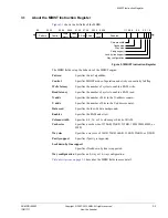
MBIST Instruction Register 

ARM DDI 0402F

Copyright © 2007-2010 ARM. All rights reserved.

3-7

ID011711

Non-Confidential

3.2.4

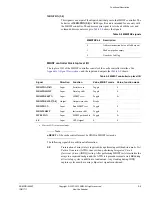
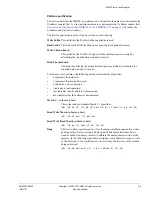
Y-address and X-address fields, MBIR[36:33] and MBIR[40:37]

You can determine the number of address bits you must specify for a RAM from the MBIR 
fields:

X-address

Y-address.

This enables you to specify your address range in two dimensions, this represents the topology 
of the physical implementation of the RAM more accurately. These two dimensions are 
controlled by two separate address counters, the X-address counter and the y-address counter. 
One counter can be incremented or decremented only when the other counter has expired. The 
chosen test algorithm determines the counter that moves faster.

Normal mode

Use this procedure to determine how many bits to assign to the X-address and Y-address 
counters: 

1.

Determine the column width of the RAM array. The Y-address must have at least that 
many bits for the column select. If it is a Data RAM, add two bits to that number for the 
doubleword select.

2.

Determine how many address bits the RAM requires. See 

Cache controller RAMs

 on 

page 3-11

. Subtract the current Y-address bit number from that number. If the result is 

eight or fewer bits, they are all assigned to the X-address for the row select. Otherwise, 
eight bits are used for the X-address and any unassigned bits are added to the bits already 
assigned to the Y-address and used for the block select.

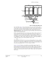
Figure 3-2 on page 3-8

 shows an example topology for the Data RAM in a 256K level-2 cache.

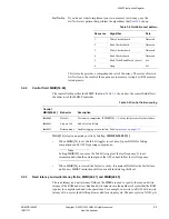
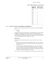
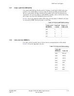
0b0101

6

0b0110

7

0b0111

8

0b1000

9

0b1001

10

0b1010

11

0b1011

12

0b1100

13

0b1101

14

0b1110

15

0b1111

16

Table 3-5 Write latency field encoding (continued)

Write latency
MBIR[48:45]

Number of cycles
per write operation

Summary of Contents for L2C-310

Page 1: ...Copyright 2007 2010 ARM All rights reserved ARM DDI 0402F ID011711 CoreLink Level 2 MBIST Controller L2C 310 Revision r3p2 Technical Reference Manual ...

Page 2: ...f merchantability or fitness for purpose are excluded This document is intended only to assist the reader in the use of the product ARM shall not be liable for any loss or damage arising from the use of any information in this document or any error or omission in such information or any incorrect use of the product Where the term ARM is used it means ARM or any of its subsidiaries as appropriate C...

Page 3: ...e MBIST controller 1 2 1 2 MBIST controller interface 1 3 1 3 RTL configuration 1 6 1 4 Product revisions 1 7 Chapter 2 Functional Description 2 1 Functional overview 2 2 2 2 Functional operation 2 11 Chapter 3 MBIST Instruction Register 3 1 About the MBIST Instruction Register 3 2 3 2 Field descriptions 3 3 Appendix A Signal Descriptions A 1 MBIST controller interface signals A 2 A 2 Miscellaneou...

Page 4: ...M All rights reserved iv ID011711 Non Confidential Preface This preface introduces the CoreLink Level 2 MBIST Controller L2C 310 Technical Reference Manual It contains the following sections About this book on page v Feedback on page viii ...

Page 5: ...ssumed Using this book This book is organized into the following chapters Chapter 1 Introduction Read this for an introduction to MBIST technology Chapter 2 Functional Description Read this for a description of the cache controller interface to the MBIST controller and MBIST testing of the data RAM and tag RAMs Also read this chapter for a description of the timing sequences for loading MBIST inst...

Page 6: ...e example code and Enclose replaceable terms for assembler syntax where they appear in code or code fragments For example MRC p15 0 Rd CRn CRm Opcode_2 Timing diagrams The figure named Key to timing diagram conventions explains the components used in timing diagrams Variations when they occur have clear labels You must not assume any timing information that is not explicit in the diagrams Shaded b...

Page 7: ...es an active LOW signal Additional reading This section lists publications by ARM and by third parties See Infocenter http infocenter arm com for access to ARM documentation ARM publications This book contains information that is specific to this product See the following documents for other relevant information AMBA AXI Protocol Specification ARM IHI 0022 ARM Architecture Reference Manual ARM DDI...

Page 8: ...upplier and give The product name The product revision or version An explanation with as much information as you can provide Include symptoms and diagnostic procedures if appropriate Feedback on content If you have comments on content then send an e mail to errata arm com Give the title the number ARM DDI 0402F the page numbers to which your comments apply a concise explanation of your comments AR...

Page 9: ... reserved 1 1 ID011711 Non Confidential Chapter 1 Introduction This chapter introduces the MBIST controller It contains the following sections About the MBIST controller on page 1 2 MBIST controller interface on page 1 3 Product revisions on page 1 7 ...

Page 10: ...y testing of the Level 2 L2 cache RAM Note The example integration files provided with the MBIST controller only support a 16 way cache design MBIST mode takes priority over all other modes for example scan testing in that the L2 RAMs are only accessible to the MBIST controller when MBIST mode is activated with the MTESTON pin You must keep the MTESTON signal LOW during functional mode and the AXI...

Page 11: ... Instead the MBIST controller uses an additional input to the existing functional multiplexors without reducing maximum operating frequency Figure 1 4 on page 1 4 shows the five pipeline stages used to access the cache RAM arrays MBISTDATAIN MBISTRESETN MTESTON MBISTDSHIFT MBISTRUN MBISTSHIFT MBISTRESULT 2 0 nRESET CLK CLK MBISTDOUT 63 0 MBISTDCTL 19 0 MBISTRESETN MTESTON MBISTDSHIFT MBISTRUN MBIS...

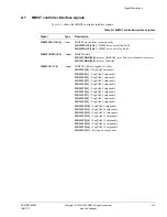
Page 12: ...ler MBIST interface signals Name Type Description nRESET Input Global active LOW reset signal CLK Input Active HIGH clock signal This clock drives the cache controller logic MBISTDOUT 63 0 Output Data out bus from all cache RAM blocks MBISTDCTL 19 0 Input Delayed versions of the MBISTCE 17 0 signal and the doubleword select signal MBISTADDR 1 0 Selects the correct read data after it passes through...

Page 13: ...cal Reference Manual for more information about the MBIST interface MBISTWE 31 0 Input Global write enable signal for all RAM arrays MBISTADDR 19 0 Input Address signal for cache RAM array MBISTADDR 1 0 is the doubleword select value See Y address and X address fields MBIR 36 33 and MBIR 40 37 on page 3 7 for a description of the doubleword select Not all RAM arrays use the full address width MBIS...

Page 14: ...mented in file logical pl310 verilog_mbist pl310MBDefs v pl310_DATA_BANKING is commented in file logical pl310 verilog pl310_defs v If you want to use the banked RAM organization both of these defines have to be uncommented The banked RAM structure splits both the Data RAM and Data parity RAM into four arrays Two dedicated L2C 310 MBIST Yaddr bits select one of the four arrays See Y address and X ...

Page 15: ...r0p0 r1p0 The difference between these revisions is additional latency cycles in MBIR See Read latency and write latency fields MBIR 44 41 and MBIR 48 45 on page 3 5 r1p0 r2p0 There is no functional difference between these two revisions r2p0 r3p0 Added support for data banking r3p0 r3p1 There is no functional difference between these two revisions r3p1 r3p2 There is no functional difference betwe...

Page 16: ...s chapter contains a functional overview and MBIST controller implementation The functional operation provides timing sequences for loading instructions starting the MBIST engine detecting failures and retrieving the data log It contains the following sections Functional overview on page 2 2 Functional operation on page 2 11 ...

Page 17: ... setup read access write access See also Compiled RAM latencies on page 2 3 You can use the MBIST controller for testing the cache controller compiled RAMs You can also choose to design your own MBIST controller You can only access one RAM by the MBIST port at a time Note For the MBIST to run correctly on the cache controller set the signals on the cache controller interface as follows set ASSOCIA...

Page 18: ...s nomenclature the shortest latency is one During functional mode the latencies for each RAM are programmed in the cache controller Auxiliary Control Register For MBIST you must know the latencies of the RAMs being tested The MBIST controller defaults to one cycle of latency but must reprogram this during the instruction load before MBIST testing can begin The latency of the current RAM being test...

Page 19: ... previous MBIST transaction you use the MBISTDCTL 1 0 signal You require separate pins because the MBIST transactions are pipelined The MBIST controller Table 2 1 Cache controller compiled RAM latency Latency bits 3 0 Cycles of latency 4 b0000 1 cycle of latency No additional latency This is the default 4 b0001 2 cycles of latency 4 b0010 3 cycles of latency 4 b0011 4 cycles of latency 4 b0100 5 c...

Page 20: ...reads from previous MBIST transactions Figure 2 3 on page 2 6 shows the cache controller MBIST paths for data RAM testing Table 2 2 MBISTADDR and MBISTDIN mapping for data RAM 8 way L2 cache size Number of data RAM indexes MBISTADDR to data RAM mapping MBISTDIN to data RAM mapping 128KB 4 096 DATAADDR 11 0 MBISTADDR 18 16 10 2 DATAWD 63 0 MBISTDIN 63 0 256KB 8 192 DATAADDR 12 0 MBISTADDR 18 16 11 ...

Page 21: ...MbistaddrD1 17 0 MbistceD1 0 MbistdinD1 63 0 MbistweD1 DATAADDR 16 0 DATACS DATAEN 31 0 DATAWD 255 0 DATARD 255 0 MbistdctlD1 2 0 MtestonD1 Data RAM LRB0 MBISTDOUT 63 0 MBISTADDR 19 0 MBISTCE 17 0 h001 MBISTDIN 63 0 MBISTDCTL 19 0 MBISTWE 31 0 MTESTON MtestonD1 64 256 Table 2 4 Writes for data RAM testing MBISTADDR 1 0 DATAEN 31 0 DATAWD used 0b00 0x000F 63 0 0b01 0x00F0 127 64 0b10 0x0F00 191 128...

Page 22: ...s for tag RAM testing Figure 2 4 Cache controller MBIST paths for tag RAM testing Note MBISTCE 16 1 corresponds to TAGCS 15 0 MDBISTDCL 18 3 corresponds to TAG 15 0 Only bits 22 0 of MBISTDIN and MBISTDOUT are used Table 2 6 MBISTADDR and MBISTDIN mapping for tag RAM 16 way L2 cache size Way size Numberof tag RAM indexes MBISTADDR to tag RAM mapping MBISTDIN to tag RAM mapping 256KB 16KB 512 TAGAD...

Page 23: ...ut of the MBIST controller that goes to the dispatch unit Table 2 7 shows the signals When the instruction shift is enabled data shifts between the two parts of the BIST engine are on bit 3 In run test mode this bit is used as invert data information The MBISTTX 11 0 interface is ARM specific and intended for use only with the MBIST controller MBIST controller Dispatch unit MBISTTX 11 0 MBISTRX 2 ...

Page 24: ...orming multiload Automatic Test Pattern Generator ATPG runs or when performing Integrated Circuit Quiescent Current IDDQ testing After performing MBIST tests to initialize the arrays to a required background the ATPG test procedures must assert SE during all test setup cycles in addition to load unload Any clocking during IDDQ capture cycles must have array chip select signals constrained Table 2 ...

Page 25: ...ection of the instruction register If bit 5 is set the MBISTRESULT 1 signal is asserted for a single cycle for each failed compare If bit 5 is not set the MBISTRESULT 1 signal is sticky and is asserted from the first failure until the end of the test At the completion of the test the MBISTRESULT 2 signal goes HIGH The MBISTRESULT 0 signal indicates that an address expire has occurred and enables y...

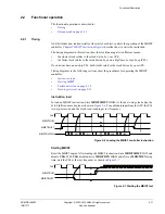
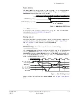
Page 26: ...the clock driven by your ATE Timing diagrams in the following sections show the procedures for operating the MBIST controller Instruction load Starting MBIST Failure detection on page 2 12 Data log retrieval on page 2 12 Instruction load To load an MBIST instruction drive MBISTSHIFT HIGH At the next rising clock edge the 61 bit shift sequence begins as shown in Figure 2 6 To enable data input from...

Page 27: ...t to generate failure statistics Figure 2 9 and Figure 2 10 on page 2 13 show the method of retrieving a data log Note MBISTRESULT 0 is the serial data output for instructions and the data log After the MBISTRESULT 2 flag goes HIGH stop the test by putting the PLL in bypass mode and driving MBISTRUN LOW as Figure 2 9 shows To begin shifting out the data log on MBISTRESULT 0 drive MBISTDSHIFT HIGH ...

Page 28: ...ing the current test and waits for you to begin shifting out the data log as Figure 2 11 shows Figure 2 11 Start of bitmap data log retrieval After you finish shifting and drive MBISTDSHIFT LOW the controller then resumes testing where it stopped as Figure 2 12 on page 2 14 shows This process continues until the test algorithm completes A fault can cause a failure to occur several times during a g...

Page 29: ...2F Copyright 2007 2010 ARM All rights reserved 2 14 ID011711 Non Confidential Figure 2 12 End of bitmap data log retrieval Loading a new instruction resets bitmap mode D 83 D 84 D 85 CLK MBISTRESULT 1 MBISTDSHIFT MBISTRESULT 0 MBISTRUN ...

Page 30: ...tial Chapter 3 MBIST Instruction Register This chapter describes how to use the MBIST Instruction Register MBIR to configure the mode of operation of the MBIST controller It contains the following sections About the MBIST Instruction Register on page 3 2 Field descriptions on page 3 3 ...

Page 31: ...ifies the number of bits in the Y address counter Data seed Specifies the four bit data background Enables Specifies the RAM under test Column width Specifies 4 8 16 or 32 columns per block of RAM Cache size Specifies a cache size of 128KB 256KB 512KB 1MB 2MB 4MB or 8MB Way size Specifies a way size of 16KB 32KB 64KB 128KB 256KB or 512KB Parity support Specifies if parity is supported Lockdown by ...

Page 32: ... specification on page 3 4 describes their use The N values in the table indicate the number of RAM accesses per address location and give an indication of the test time when using that algorithm Table 3 1 Pattern field encoding Pattern MBIR 60 55 Algorithm name N Description 0b000000 Write Solids 1N Write a solid pattern to memory 0b000001 Read Solids 1N Read a solid pattern from memory 0b000010 ...

Page 33: ... created by alternating the supplied data seed and its inverse For the next set of patterns the following notation describes the algorithm 0 represents the data seed 1 represents the inverse data seed w indicates a write operation r indicates a read operation incr indicates that the address is incremented decr indicates that the address is decremented March C x fast or y fast This is the industry ...

Page 34: ...est frequency When MBIR 54 is cleared the fail bit is sticky It remains HIGH after the first failure until a new MBIST instruction shifts in or until the data log shifts out 3 2 3 Read latency and write latency fields MBIR 44 41 and MBIR 48 45 The read latency and write latency fields of the MBIR are used to specify the read and write latency of the RAM under test Read and write latencies are the ...

Page 35: ...ou must still program both the read latency and write latency fields of the MBIR with the same value Table 3 4 shows the latency settings for read operations Table 3 5 shows the latency settings for write operations Table 3 4 Read latency field encoding Read latency MBIR 44 41 Number of cycles per read operation 0b0000 1 0b0001 2 0b0010 3 0b0011 4 0b0100 5 0b0101 6 0b0110 7 0b0111 8 0b1000 9 0b100...

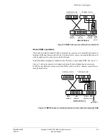
Page 36: ...w many bits to assign to the X address and Y address counters 1 Determine the column width of the RAM array The Y address must have at least that many bits for the column select If it is a Data RAM add two bits to that number for the doubleword select 2 Determine how many address bits the RAM requires See Cache controller RAMs on page 3 11 Subtract the current Y address bit number from that number...

Page 37: ...MBIR 36 33 0b0111 and the X address field must have a value of eight MBIR 40 37 0b1000 Values higher or lower than these produce incorrect results Note If the columns have fewer than 256 rows you must still assign address bits to the row address until all eight bits are used before assigning any to the block address If the cache RAM has more than 256 rows per column then the additional bits must b...

Page 38: ...ping for banked RAM is the same as non banked RAM See Figure 3 3 Figure 3 4 shows the structure for banked mode data RAM and banked mode data parity RAM The only difference from normal mode RAM is that two of the Y address counter bits now form the Bank select Figure 3 4 MBIST address scrambling for banked mode data and data parity RAM 0 1 0 1 9 2 3 7 6 5 4 3 2 1 0 X address counter Y address coun...

Page 39: ...es the number of X address counter bits to use during test Table 3 7 shows the X address settings Table 3 6 Y address field encoding Y address MBIR 36 33 Number of counter bits 0b0010 Unsupported 0b0010 2 0b0011 3 0b0100 4 0b0101 5 0b0110 6 0b0111 7 0b1000 8 0b1001 9 0b1010 10 0b1010 Reserved Table 3 7 X address field encoding X address MBIR 40 37 Number of counter bits 0b0010 Unsupported 0b0010 2...

Page 40: ...10 shows the required sums of the X address and Y address fields for testing of data parity RAM Table 3 8 Required sums of X address and Y address fields for data RAM Cache size Data RAM 128KB 14 256KB 15 512KB 16 1MB 17 2MB 18 4MB 19 8MB 20 Table 3 9 Required sums of X address and Y address fields for tag RAM Way size Tag RAM 16KB 9 32KB 10 64KB 11 128KB 12 256KB 13 512KB 14 Table 3 10 Required s...

Page 41: ...o give the full 64 bits of data required on the MBISTDIN 63 0 port of the MBIST interface 3 2 6 Enables field MBIR 28 11 Table 3 11 shows how each bit in the enables field selects the cache RAM array to be tested You can select only one array at a time Selecting multiple arrays produces unpredictable behavior Table 3 11 Enables field encoding Enables MBIR 28 11 RAM name 0b000000000000000001 Data 0...

Page 42: ... line stress testing and writing a true physical checkerboard pattern to the array Table 3 12 shows the supported column widths along with the number of LSB address bits used for each and the MBIR encodings required to select them 3 2 8 Cache size field MBIR 8 6 The cache size field specifies the size of the cache in your implementation of the module Table 3 13 shows the supported cache sizes Tabl...

Page 43: ...tion Set to 1 if parity is enabled 3 2 11 Lockdown by line support field MBIR 1 The lockdown by line support field specifies if lockdown by line is supported in your implementation Set to 1 if lockdown by line is enabled 3 2 12 Way configuration field MBIR 0 The way configuration field specifies an 8 way or 16 way configuration in your implementation Set to 0 for an 8 way configuration or 1 for a ...

Page 44: ...ights reserved A 1 ID011711 Non Confidential Appendix A Signal Descriptions This appendix describes the MBIST controller signals It contains the following sections MBIST controller interface signals on page A 2 Miscellaneous signals on page A 4 ...

Page 45: ...as doubleword select MBISTADDR 14 2 used for Tag RAM MBISTCE 17 0 Output MBIST RAM chip enables for writes MBISTCE 0 Data RAM chip enable MBISTCE 1 Tag RAM 0 chip enable MBISTCE 2 Tag RAM 1 chip enable MBISTCE 3 Tag RAM 2 chip enable MBISTCE 4 Tag RAM 3 chip enable MBISTCE 5 Tag RAM 4 chip enable MBISTCE 6 Tag RAM 5 chip enable MBISTCE 7 Tag RAM 6 chip enable MBISTCE 8 Tag RAM 7 chip enable MBISTC...

Page 46: ...MBIST RAM select for Tag RAM 10 MBISTDCTL 14 MBIST RAM select for Tag RAM 11 MBISTDCTL 15 MBIST RAM select for Tag RAM 12 MBISTDCTL 16 MBIST RAM select for Tag RAM 13 MBISTDCTL 17 MBIST RAM select for Tag RAM 14 MBISTDCTL 18 MBIST RAM select for Tag RAM 15 MBISTDCTL 19 MBIST RAM select for data parity MBISTDIN 63 0 Output MBIST Data In to cache controller MBISTDIN 63 0 MBIST data in for Data RAM M...

Page 47: ...neous signals Table A 2 Miscellaneous signals Signal Type Description nRESET Input Global active LOW reset signal CLK Input Clock MBISTDATAIN Input Serial data in MBISTDSHIFT Input Data log shift MBISTRESETN Input MBIST reset MBISTRESULT 2 0 Output Output status bus MBISTRUN Input Run MBIST test MBISTSHIFT Input Instruction shift MTESTON Input MBIST Mode Enable ...

Page 48: ...issue C and issue D Change Location Affects RAM organization updated RTL configuration on page 1 6 Banked RAM organization on page 3 9 Table 3 10 on page 3 11 r3p0 Table B 2 Differences between issue D and issue E Change Location Affects MBIST controller interface description updated MBIST controller interface on page 2 2 r3p1 Table B 3 Differences between issue E and issue F Change Location Affec...

Page 49: ...tion Specific Integrated Circuit ASIC An integrated circuit that has been designed to perform a specific application function It can be custom built or mass produced Architecture The organization of hardware and or software that characterizes a processor and its attached components and enables devices with similar characteristics to be grouped together when describing their behavior for example Ha...

Page 50: ...rom 0 to number of lines per way 1 See also Cache terminology diagram on the last page of this glossary Cache lockdown To fix a line in cache memory so that it cannot be overwritten Cache lockdown enables critical instructions and or data to be loaded into the cache so that the cache lines containing them are not subsequently reallocated This ensures that all subsequent accesses to the instruction...

Page 51: ... is the circuitry in a computer system required to process data using the computer instructions It is an abbreviation of microprocessor A clock source power supplies and main memory are also required to create a minimum complete working computer system Physical Address PA The MMU performs a translation on Modified Virtual Addresses MVA to produce the Physical Address PA which is given to AHB to pe...

Page 52: ...o be discarded to make room for a replacement cache line that is required as a result of a cache miss The way in which the victim is selected for eviction is processor specific A victim is also known as a cast out Way See Cache way WB See Write back Word A 32 bit data item Write Writes are defined as operations that have the semantics of a store That is the ARM instructions SRS STM STRD STC STRT S...

Page 53: ...the cache is updated WT See Write through Cache terminology diagram The diagram below illustrates the following cache terminology block address cache line cache set cache way index tag Block address Tag Tag Tag Tag Index Word Hit way number Read data way that corresponds 3 1 Tag 0 0 2 1 3 4 5 6 7 n Byte Cache way Cache set m 1 2 0 Cache line 2 Line number Word number Cache tag RAM Cache data RAM ...

Reviews: