Introduction
ARM DDI 0402F
Copyright © 2007-2010 ARM. All rights reserved.
1-5
ID011711
Non-Confidential
Note
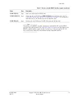
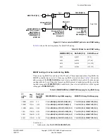
The interface of the MBIST controller communicates with both the ATE and the MBIST
interface of the cache controller. See
Appendix A
Signal Descriptions
for descriptions of the
MBIST controller interface signals. See the
CoreLink Level 2 Cache Controller L2C-310
Technical Reference Manual
for more information about the MBIST interface.
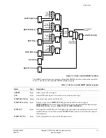
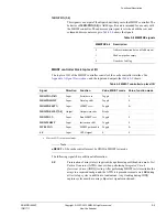
MBISTWE[31:0]
Input
Global write enable signal for all RAM arrays.
MBISTADDR[19:0]
Input
Address signal for cache RAM array.
MBISTADDR[1:0]
is the doubleword select value. See
Y-address and X-address fields, MBIR[36:33] and MBIR[40:37]
on page 3-7
for a description of
the doubleword select. Not all RAM arrays use the full address width.
MBISTDIN[63:0]
Input
Data bus to the cache RAM arrays. Not all RAM arrays use the full data width.
Table 1-1 Cache controller MBIST interface signals (continued)
Name
Type
Description

