2003 Microchip Technology Inc.
Preliminary
DS41206A-page 49
PIC16F716
8.0
ANALOG-TO-DIGITAL
CONVERTER (A/D) MODULE
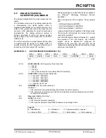
The Analog-to-Digital (A/D) Converter module has four
inputs.
The A/D allows conversion of an analog input signal to
a corresponding 8-bit digital number (refer to
Application Note AN546 for use of A/D Converter). The
output of the sample and hold is the input into the
converter, which generates the result via successive
approximation. The analog reference voltage is
software selectable to either the device’s positive
supply voltage (V
DD
) or the voltage level on the RA3/
AN3/V
REF
pin.
The A/D converter has a unique feature of being able
to operate while the device is in Sleep mode. To
operate in Sleep, the A/D conversion clock must be
derived from the A/D’s internal RC oscillator.
Additional information on the A/D module is available in
the PICmicro
®
Mid-Range Reference Manual,
(DS33023).
The A/D module has three registers. These registers
are:
• A/D Result Register (ADRES)
• A/D Control Register 0 (ADCON0)
• A/D Control Register 1 (ADCON1)
A device Reset forces all registers to their Reset state.
This forces the A/D module to be turned off and any
conversion is aborted.
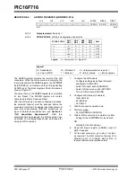
The ADCON0 register, shown in Register 8-1, controls
the operation of the A/D module. The ADCON1
register, shown in Register 8-2, configures the
functions of the port pins. The port pins can be
configured as analog inputs (RA3 can also be a voltage
reference) or as digital I/O.
REGISTER 8-1:
ADCON0 REGISTER (ADDRESS: 1Fh)
R/W-0
R/W-0
R/W-0
R/W-0
R/W-0
R/W-0
R/W-0
R/W-0
ADCS1
ADCS0
CHS2
CHS1
CHS0
GO/DONE
—
ADON
bit 7
bit 0
bit 7-6
ADCS1:ADCS0: A/D Conversion Clock Select bits
00
= F
OSC
/2
01
= F
OSC
/8
10
= F
OSC
/32
11
= F
RC
(Clock derived from the internal ADC RC oscillator)
bit 5-3
CHS2:CHS0: Analog Channel Select bits
000
= channel 0, (RA0/AN0)
001
= channel 1, (RA1/AN1)
010
= channel 2, (RA2/AN2)
011
= channel 3, (RA3/AN3)
1xx
= reserved, do not use
bit 2
GO/DONE: A/D Conversion Status bit
If ADON = 1
1
= A/D conversion in progress (Setting this bit starts the A/D conversion)
0
= A/D conversion not in progress (This bit is automatically cleared by hardware when the A/D
conversion is complete)
bit 1
Reserved: Maintain this bit as '
0
'
bit 0
ADON: A/D On bit
1
= A/D converter module is operating
0
= A/D converter module is shutoff and consumes no operating current
Legend:
R = Readable bit
W = Writable bit
U = Unimplemented bit, read as ‘
0
’
-n = Value at POR
‘1’ = Bit is set
‘0’ = Bit is cleared
x = Bit is unknown
Summary of Contents for PIC16F716
Page 6: ...PIC16F716 DS41206A page 4 Preliminary 2003 Microchip Technology Inc NOTES...
Page 35: ......
Page 56: ......
Page 60: ......
Page 88: ......
Page 92: ...PIC16F716 DS41206A page 90 Preliminary 2003 Microchip Technology Inc NOTES...
Page 108: ...PIC16F716 DS41206A page 106 Preliminary 2003 Microchip Technology Inc NOTES...
Page 110: ...PIC16F716 DS41206A page 108 Preliminary 2003 Microchip Technology Inc NOTES...
Page 124: ...PIC16F716 DS41206A page 122 Preliminary 2003 Microchip Technology Inc NOTES...

