GeForce GTX 980 Whitepaper
GM204 HARDWARE ARCHITECTURE
IN-DEPTH
8
from 32 to 64. Again, thanks to the added benefit of higher clocks, pixel fill-rate is actually more than
double that of GTX 680: 72 Gpixels/sec for GTX 980 versus 32.2 Gpixels/sec for GTX 680.
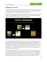
The memory subsystem has also been significantly revamped. GTX 980’s memory clock is over 15%
higher than GTX 680, and GM204’s cache is larger and more efficient than Kepler’s design, reducing the
number of memory requests that have to be made to DRAM. Improvements in our implementation of
memory compression provide a further benefit in reducing DRAM traffic—effectively amplifying the raw
DRAM bandwidth in the system.
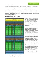
Maxwell Streaming Multiprocessor
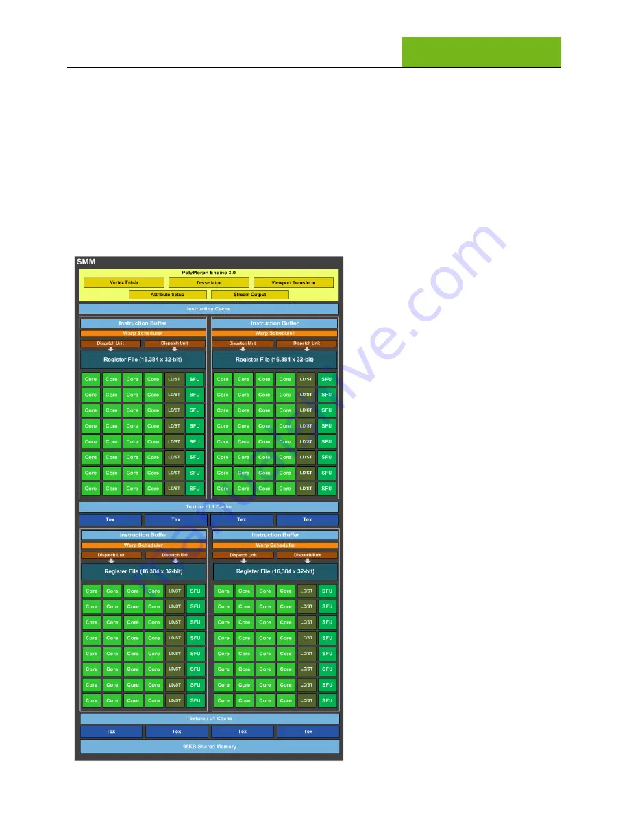
The SM is the heart of our GPUs. Almost
every operation flows through the SM at
some point in the rendering pipeline.
Maxwell GPUs feature a new SM that’s
been designed to provide dramatically
improved performance per watt than prior
GeForce GPUs.
Compared to GPUs based on our Kepler
architecture, Maxwell’s new SMM design
has been reconfigured to improve
efficiency. Each SMM contains four warp
schedulers, and each warp scheduler is
capable of dispatching two instructions per
warp every clock.
Compared to Kepler’s
scheduling logic, we’ve integrated a
number of improvements in the scheduler
to further reduce redundant re-
computation of scheduling decisions,
improving energy efficiency. We’ve also
integrated a completely new datapath
organization. Whereas Kepler’s SM shipped
with 192 CUDA Cores—a non-power-of-two
organization—the Maxwell SMM is
partitioned into four distinct 32-CUDA core
processing blocks (128 CUDA cores total
per SM), each with its own dedicated
resources for scheduling and instruction
buffering. This new configuration in
Maxwell aligns with warp size, making it
easier to utilize efficiently and saving area
Figure 3: GM204 SMM Diagram (GM204 also features 4 DP units per
SMM, which are not depicted on this diagram)


