LTE Standard Module Series
In short frame mode, the data is sampled on the falling edge of the PCM_CLK and transmitted on the
rising edge. The PCM_SYNC falling edge represents the MSB. In this mode, the PCM interface supports
256 kHz, 512 kHz, 1024, 2048 kHz PCM_CLK at 8 kHz PCM_SYNC, and also supports 4069 kHz
PCM_CLK at 16 kHz PCM_SYNC.
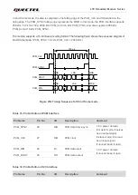
The module supports a 16-bit linear encoding format. The following figure shows the sequence diagram of
short frame mode.
(PCM_SYNC = 8 kHz, PCM_CLK = 2048 kHz).
PCM_CLK
PCM_SYNC
PCM_DOUT
MSB
LSB
MSB
125 µs
1
2
256
255
PCM_DIN
MSB
LSB
MSB
Figure 21
:
Timing Sequence for Short frame mode
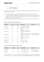
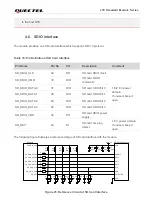
Table 15: Pin Definition of PCM Interface
Table 16: Pin Definition of I2C Interface
Pin Name
Pin No.
I/O
Description
Comment
PCM_SYNC
26
DIO
PCM data frame sync
1.8 V power domain.
In master mode, it serves
as an output signal.
In slave mode, it is used
as an input signal.
If unused, keep it open.
PCM_CLK
27
DIO
PCM clock
PCM_DIN
24
DI
PCM data input
1.8 V power domain.
If unused, keep it open.
PCM_DOUT
25
DO
PCM data output
Pin Name
Pin No.
I/O
Description
Comment

