6.6.4
Analog input
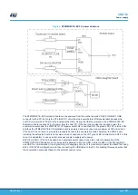
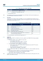
The CN21 two-pin header and RV3 10 KΩ potentiometer are connected to PB2 of MCU as analog input. A
low
‑
pass filter can be implemented by replacing R104 and C81 with the right value of resistor and capacitor as
requested by the end user’s application.
6.6.5
External I
2
C connector
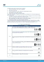
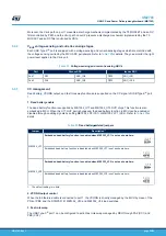
The I2C1 bus of the MCU is connected to CN4 on the STM32G0C1E-EV Evaluation board. The I
2
C functional
daughterboard can be mounted on the CN4 connector and accessed by the microcontroller through the I2C1
bus. It shares the same I2C1 bus with the U3 temperature sensor and DDC on the MB1351_CN3 HDMI_Source
connector on the legacy peripheral daughterboard.
The pull-up voltage level of the I2C1 bus is automatically decided by the daughterboard (the legacy peripheral
daughterboard or the UCPD daughterboard) on CN2 and CN3. If there is no daughterboard on these connectors,
pin 17 and pin 18 must be shortened on CN2 and CN3 by jumpers. Thus I
2
C and reset pull-up voltages on CN4
are the voltage of VDD.
6.6.6
Motor control
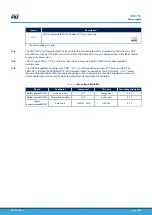
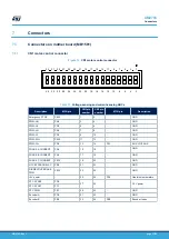
The STM32G0C1E-EV Evaluation board supports both asynchronous and synchronous three-phase brushless
motor control via the CN1 34-pins connector, which provides all required control and feedback signals to and from
the motor power driving board. Available signals on this connector include emergency stop, motor speed, 3-phase
motor current, bus voltage, power heatsink temperature coming from the motor driving board, and six channels of
PWM control signal going to the motor driving circuit. The daughterboard on CN2 and CN3 must be removed and
some jumpers set for motor-control application:
•
JP5, JP6, and JP7 jumpers ON
•
JP22 and JP19 jumpers OFF
•
JP13[2-3] and JP15[2-3] jumpers OFF.
6.6.7
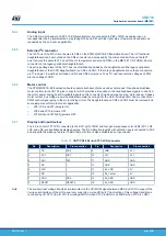
Display and input devices
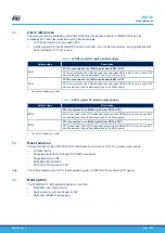
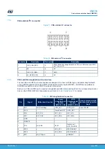
The 2.4-inch color TFT LCD connected to the SPI1 port of MCU and four general
‑
purpose color LEDs (LD1, LD2,
LD3, and LD4) are available as display devices. The B3 4-direction joystick with selection key is connected to PA0
and supports the wake-up feature. The B2 Tamper button is also available as an input device.
Table 13.
CN17/CN19 2.4-inch TFT-LCD connector
Pin
Description
Pin connection
Pin
Description
Pin connection
1
CS
PB8
9
VDD
3.3V
2
SCL
PB3
10
VCI
3.3V
3
SDI
PA7
11
GND
GND
4
RS
-
12
GND
GND
5
WR
-
13
BL_VDD
5V
6
RD
-
14
BL_Control
5V
7
SDO
PB4
15
BL_GND
GND
8
RESET
RESET#
16
BL_GND
GND
Note:
The bi-directional voltage translator implemented on the SPI MOSI signal between MCU and LCD to support the
3-wire serial interface of the LCD panel only supports a 3-wire SPI port. The direction of this voltage translator is
controlled by I/O PC12 (the IO PA7 is working as MOSI when PC12 is HIGH or as MISO when PC12 is LOW).
UM2783
Peripherals on mother board (MB1581)
UM2783
-
Rev 1
page 20/59

