


Virtex-6 FPGA System Monitor
11
UG370 (v1.1) June 14, 2010
Analog-to-Digital Converter
are overwritten when a full chip configuration is carried out. To enable auxiliary analog
input channels during preconfiguration, see
.
Because no system clock is available, System Monitor uses an internal clock oscillator
pre-configuration. The full functionality of System Monitor is accessed pre-configuration
through the JTAG Test Access Port (JTAG TAP) (see
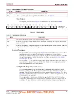
The JTAG interface provides full Read/Write access to the System Monitor register file
interface. After power-up, the System Monitor functionality is customized, if required,
through the JTAG TAP. The System Monitor functionality is also available through the
JTAG TAP post configuration even if System Monitor has not been instantiated in a design.
It is possible to access the System Monitor registers at any time using the JTAG TAP.
The basic connection requirements that ensure the System Monitor functionality is enabled
are shown in
. For more information regarding power supply requirements, see
Application Guidelines, page 45
Analog-to-Digital Converter
The ADC is used to digitize the output of the on-chip sensors and voltages connected to
the external analog inputs. The ADC specifications are listed in the
Virtex-6 FPGA Data
Sheet
.
The System Monitor ADC carries out a 16-bit resolution conversion of all sensor and
external analog input voltages. However, only 10-bit performance is specified and
guaranteed in the
Virtex-6 FPGA Data Sheet
. These additional conversion bits are accessable
to improve the resolution of a measurement on an external channel. A more detailed
discussion can be found in
Application Guidelines, page 45
. Since the ADC has a specified
performance of 10-bits and to simplify the discussion, a 10-bit transfer function is used in
this guide to illustrate operation.
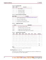
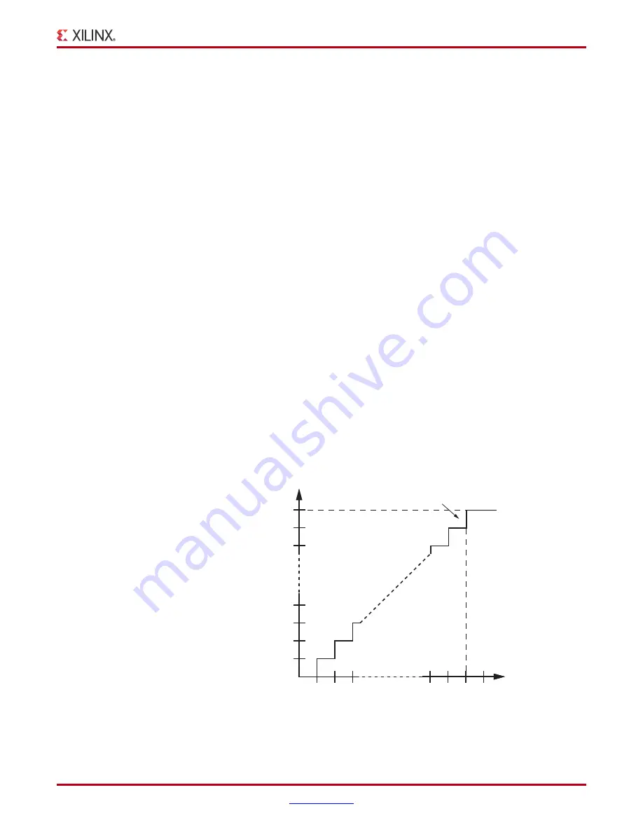
The 10-bit full scale output code of
3FFh
is produced when a 1V differential voltage is
placed on an external analog input (see
).
X-Ref Target - Figure 3
Figure 3:
ADC Transfer Function
000
001
003
004
3FF
Output Code
Full Scale
Transition
3FE
3FD
002
1
2
3
999
Full Scale Input = 1V
1 LSB = 1V / 1024 = 977
μ
V
10-Bit Output Code (He
x)
UG370_03_
060709
Input Voltage (mV)
www.BDTIC.com/XILINX


