14
Virtex-6 FPGA System Monitor
UG370 (v1.1) June 14, 2010
Register File Interface
Power Supply Sensor
System Monitor also includes on-chip sensors allowing a user to monitor the FPGA power-
supply voltages using the ADC. The sensors sample and attenuate (by a factor of three) the
power supply voltages V
CCINT
and V
CCAUX
on the package power supply balls.
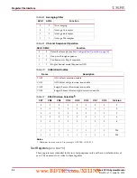
shows the power-supply sensor transfer function after digitizing by the ADC. The Power
Supply sensor can be used to measure voltages in the range 0V to V
CCAUX
+ 5% with a
resolution of approximately 3 mV:
Supply Voltage (Volts) = (ADC Code / 1024) x 3V
Equation 3
Similar to the temperature sensor, System Monitor provides a digital-averaging function
for the power supply measurements. Thus, up to 256 measurements of a sensor output are
used to generate a single reading. The power-supply measurement results for V
CCINT
and
V
CCAUX
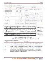
are stored in the data registers at DRP addresses
01h
and
02h
, respectively (see
).
Register File Interface
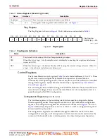
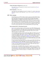
illustrates the System Monitor register file interface. All registers in the register
file interface are accessible through the DRP. The DRP can be accessed via a fabric port or
the JTAG TAP. Access is governed by an arbitrator (see
). The
DRP allows the user to access up to 128 16-bit registers (DADDR[6:0] =
00h
to
7Fh
) from
the FPGA logic. The first 64 access locations (DADDR[6:0] =
00h
to
3Fh
) are read-only and
contain the status registers (see
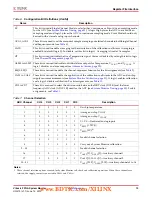
). The Control registers are located at
addresses
40h
to
7Fh
(see
) and are readable or writable via the
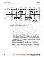
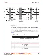
DRP. The DRP timing is shown in
. For a detailed description of the DRP
timing please refer to the
Virtex-6 FPGA Configuration Guide
. For more information on the
JTAG DRP interface, see
.
X-Ref Target - Figure 6
Figure 6:
Ideal Power Supply Transfer Function
10-Bit Output Code
Supply Voltage (Volts)
Output Code
Full Scale
Transition
2.93 mV
5.86 mV
8.79 mV
1.00V
2.50V
2.997V
2.994V
1 LSB = 2.93 mV
000h
001h
003h
004h
3FFh
3FEh
355h
155h
002h
UG370_06_
060709
www.BDTIC.com/XILINX


