ACCES I/O Products, Inc.
MADE IN THE USA
PCIe-ADIO16-16F Family Manual
9
Rev B3d
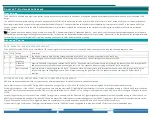
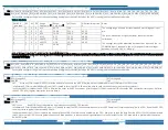
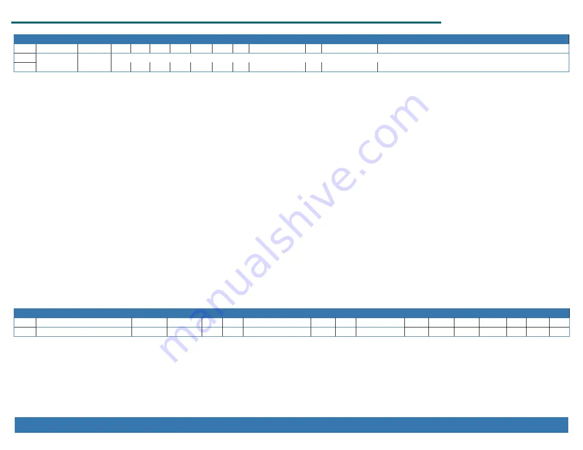
ADC FIFO Data, 30 of 32-bit Memory BAR[1]Read-Only 32-bits only
bit D31
D30
D29 D28 D27 D26 D25 D24 D23 D22 through D20 D19 D18 through D16 D15 through D0
Name INVALID=1 RUNNING UNUSED
0 (“VALID”) RSV
DIO1 DIO0 RSV RSV TEMP MUX SEQ Channel2:0
Diff Gain2:0
ADC Counts (Two’s complement)
ADC FIFO Data: Read the RAW-format ADC Conversion results (in twos-complement 16-bit form) and the associated status word.
INVALID:
If INVALID is SET then all other bits are undefined, and the entry should be discarded. This can occur if you read from the ADC FIFO while the ADC FIFO Count
(+28) is zero.
RUNNING:
SET indicates the ADC Sequencer is operating, taking either periodic (timer-driven) conversions or via the external ADC Start secondary digital function.
DIO1:0:
These bits indicate the state of the corresponding digital I/O pin at the time the paired ADC Conversion was sampled.
TEMP:
If TEMP is SET the ADC Counts are acquired from the ADAS3022’s onboard temperature sensor rather than from an analog input channel. Refer to ADC Control
(+38) for more information about acquiring the temperature data.
MUX:
If MUX is SET the ADC Counts are acquired from the ADAS3022’s Auxiliary Mux inputs rather than from the normal Analog Input Channels. Note, the PCIe-
ADIO16-16F does not have anything usefully connected to the Aux Mux inputs and you should not bother acquiring data from them.
SEQ:
The SEQ bit indicates which ADC the data is from, and can be thought of as Channel:3. That is, if SEQ is set add +8 to the channel reported by the Channel2:0
bits.
Channel2:0:
The 3 Channel bits indicate from which Analog Input the paired ADC Counts were sampled. Refer to ADC Control (+38) for important information about the
Channel bits re Differential operation.
Diff:
SET indicates the paired ADC Counts were sampled in Differential mode. Refer to ADC Control (+38) for important information about the Channel bits re
Differential operation.
Gain2:0:
The 3 Gain bits indicate at what gain code the paired ADC Counts were sampled. Refer to the gain code table in ADC Advanced Sequencer Gain Control (+18)
for how to interpret the Gain bits.
ADC Counts:
16-bit two’s complement ADC counts, the ADC conversion result from the samples Channel at the specified Gain, sampled in Differential or Singled-ended /
Pseudo-Differential mode as indicated by the Diff bit (D19).
Please refer to the “Software Tips” section for details on how to translate RAW-format ADC data into Volts — or skip the hassle and use our AIOAIO.dll API Library:
ADC_GetImmediateV(iBoard, pVolts, iChannel, iRange);, ADC_GetImmediateScanV(iBoard, pVolts[]); etc.
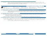
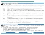
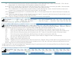
ADC Control, 38 of 32-bit Memory BAR[1]Read/Write 32-bits only
bit D31 through D19
D18
D17
D16 D15 D14 through D12
D11
D10 D9 through D7 D6
D5
D4
D3
D2
D1
D0
Name UNUSED
SCAN
CONFIG
GO
RSV IN
x
2:0
COM RSV Gain2:0
/MUX SEQ1 SEQ0 /TEMP RSV CMS RSV
Controls ADAS #0, channels 0-7
The ADAS3022 is a very flexible ADC module and we highly recommend you use the AIOAIO.dll-provided API to avoid needing to know the following information.
SCAN: If SCAN is set (to 1)
AND
INx2:0 is non-zero then each “ADC Start” event will acquire channels 0 through INx2:0 at the rate specified in +14.
CONFIG: If CONFIG is set then the ADC control bits (D15 through D0 of this register) will be written to the ADAS3022
GO:
If GO is set then, if +10 is non-zero the card will begin taking ADC conversions or scans at the rate set via +10; if +10 is zero then a single ADC conversion or scan will be
taken.
INx2:0: INx specifies the individual channel to convert (in non-sequenced modes) or the last channel of the 0-INx sequence to be converted.

