ACCES I/O Products, Inc.
MADE IN THE USA
PCIe-ADIO16-16F Family Manual
11
Rev B3d
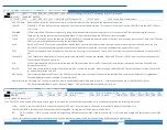
Read DIO Data to read the digital input pins or to readback the last commanded digital output state.
Write to DIO Data to configure the digital pin(s)’ high/low state for those bits in I/O Groups configured as Outputs. SET bits will output high voltage, CLEAR bits will output GND.
Refer to DIO Control (+48) for how to configure the input vs output direction of each I/O Group.
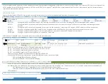
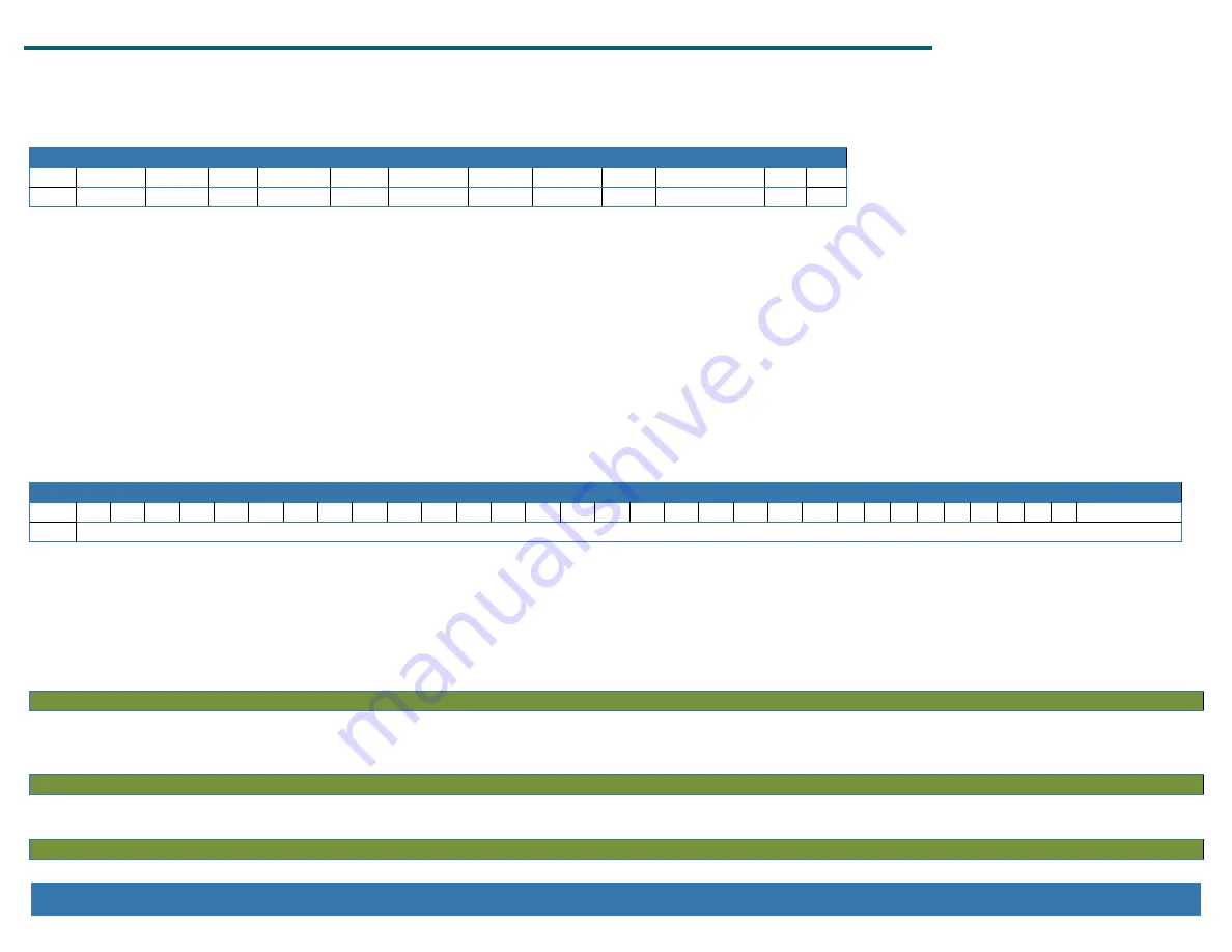
DIO Control, 48 of 64-bit Memory BAR[2+3] Read/Write 32-bits only
bit D31…D24 D23
D22
D21
D20
D19
D18
D17
D16
D15 through D8 D1
D0
Name UNUSED edgeEXT enEXT edgeLDAC enLDAC edgeSTART enSTART edgeTRIG enTRIG
unused
IOG1 IOG0
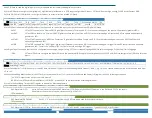
Write DIO Control to enable Digital Secondary Functions, and to control the input vs output direction of each Digital I/O Group.
enEXT:
SET enEXT to enable the “External IRQ” Digital Input Secondary Function on DIO 13 so the selected edge on the input will (optionally) generate IRQs.
enLDAC:
SET enLDAC to enable the “External LDAC” Digital Input Secondary Function on DIO12 so the selected edge will cause the DACs to update and optionally
generate an IRQ.
enSTART:
SET enSTART to enable the “ADC Start Conversion” Digital Input Secondary Function on DIO 14 so the selected edge will cause an ADC Start Event and
optionally generate an IRQ.
enTRIG:
SET enTRIG to enable the “ADC Trigger” Digital Input Secondary Function on DIO15 so the selected edge will trigger timed ADC conversions and optionally
generate an IRQ. Consult the “Software Tips” section for details on using ADC Trigger.
Each Digital Input Secondary function has a configurable active edge, rising or falling. SET the corresponding edge
XXX
bit to select rising edge, CLEAR the bit for falling edge.
IOG
x
:
SET each IOGx bit to configure the digital I/O bits in the associated I/O Group for use as digital outputs. CLEAR an IOG
x
bit to configure the I/O Group for use as
inputs.
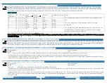
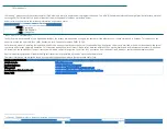
Watchdog Control, 4C of 64-bit Memory BAR[2+3] Read/Write 32-bits only
bit D31 D30 D29 D28 D27 D26 D25 D24 D23 D22 D21 D20 D19 D18 D17 D16 D15 D14 D13 D12 D11 D10 D9 D8 D7 D6 D5 D4 D3 D2 D1 D0
Name Watchdog Timeout
Write the number of Ticks (which occur at the ADC Base Clock Rate (+C)) before the Watchdog should timeout (“Bark”); e.g., for a one-second timeout period write the value read from
+C to +4C.
When the Watchdog Barks the board is RESET as if just powered on (or as if a 1 is written to the Resets and Power (+0) register) with the following exceptions:
The “WDT Output Status” output on pin 68 asserts 0.
Bit D31 of the IRQ Enable/Clear and Status (+40) “WDG” is latched SET to indicate that the Watchdog timed out.
Write 0 to the Watchdog Timeout (+4C) register to disable the Watchdog Feature.
DAC Waveform FIFO, 50 of 64-bit Memory BAR[2+3] Read/Write 32-bits only
DAC Waveform FIFO:
Write DAC commands to load the DAC Waveform FIFO. Generally 0x000nCCCC where n is the DAC# and CCCC is the counts.
Read returns the number of control values currently in the FIFO.
FDS models only
DAC Waveform DACs/Point, 54 of 64-bit Memory BAR[2+3] Read/Write 32-bits only
DAC Waveform DACs/Point:
Write 1, 2, 3 or 4 to specify how many DACs are being used for Waveform Playback.
FDS models only
DAC Waveform FIFO Size, 58 of 64-bit Memory BAR[2+3] Read 32-bits only
DAC Waveform FIFO Size: Read to determine the DAC Waveform FIFO size in 32-bit DAC command values. Typically 0x2000, or 8192 values.

