AVME941X/946X DIGITAL I/O BOARDS
_________________________________________________________________________________
- 13
-
2.9.2 Contact Closures And Switches
When sensing contact closures that already are connected to a voltage source the pullup resistor networks should
be removed. The input voltage should be within the range listed in Specifications, Section 6. For isolated or
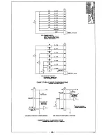
grounded contacts the pullups and the +5 volt supply can be used to establish an input voltage. See figure 2.8
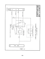
Relay Driver and Input Configurations, for various input configurations.
This chapter provides the specific information necessary to program the
Digital I/O Board.
3.0 PROGRAMMING INFORMATION
3.1 The Digital I/O Memory Map
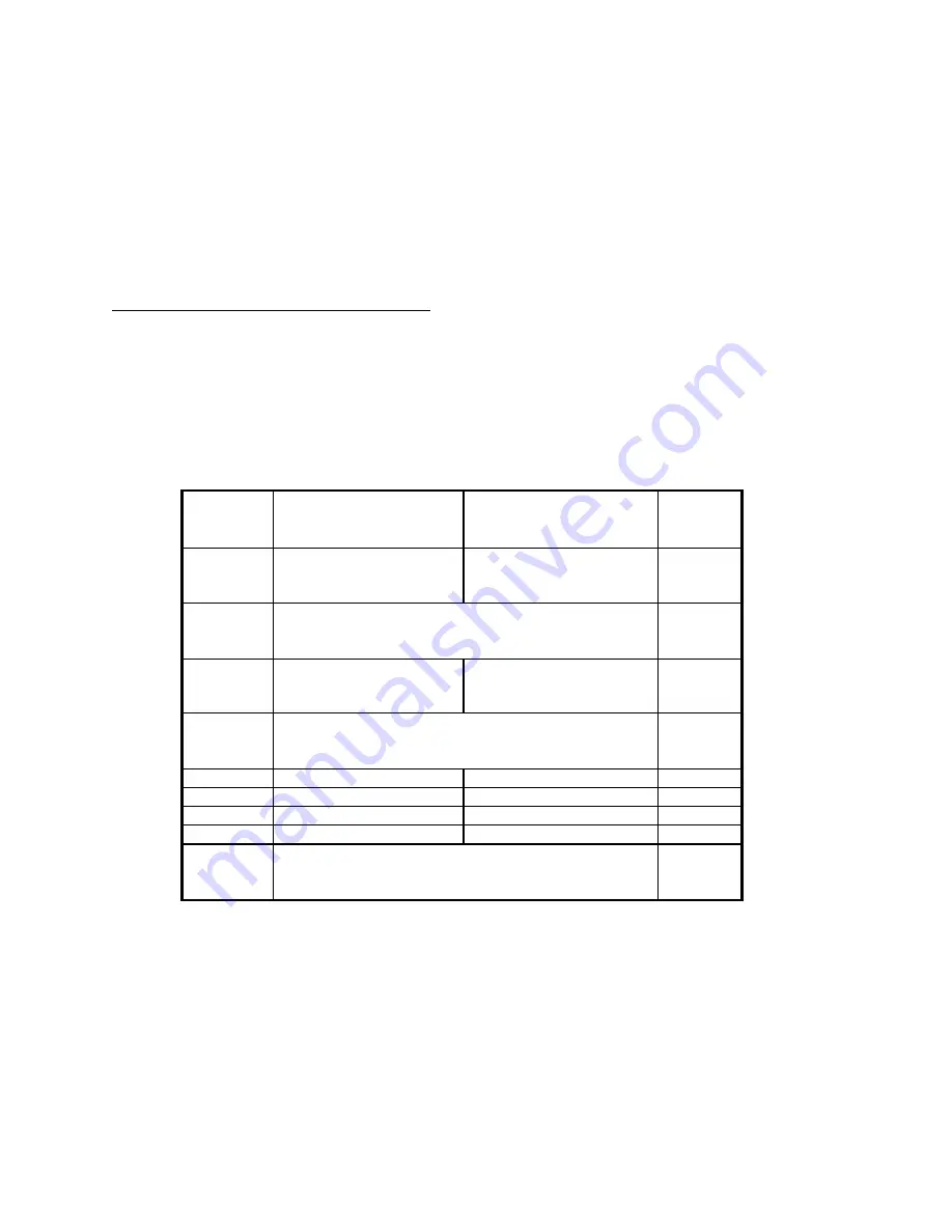
The memory map for the Digital I/O Board, a Non-Intelligent I/O architecture is shown in Figure 3.1. All addresses
are in hexadecimal. The letters R and W indicates whether a register may be read and/or written to. The areas
marked "undefined" in the memory map are reserved for future use. To allow future compatibility, application
programs must not use these areas.
Figure 3.1 AVME94XX Digital I/O Board Memory Map.
Address
Base +
(HEX)
Even
Odd
Address
Base +
(HEX)
00
↓
3E
Undefined
R - Module ID PROM
01
↓
3f
40
↓
7E
Undefined
41
↓
7F
80
Undefined
R/W - Status/Control
81
82
↓
FE
Undefined
83
↓
FF
100
R/W - I/O Port 0
R/W - I/O Port 1
101
102
R/W - I/O Port 2
R/W - I/O Port 3
103
104
R/W - I/O Port 4
R/W - I/O Port 5
105
106
R/W - I/O Port 6
R/W - I/O Port 7
107
108
↓
3FE
Undefined
109
↓
3FF
Note: For AVME 941X I/O Ports 0-7 are Write Only.
Note: Ports 4 through 7 present only on Models AVME 9410, 9411,9460, 9461.


