AVME941X/946X DIGITAL I/O BOARDS
_________________________________________________________________________________
- 16
-
relays and switches. A logic "1" in the computer produces a low level at the output driver to "pull in" a relay and
turn something "on", etc.
Reset Conditions: All of the I/O points are set to "0" which causes the output drivers to go into an off (hi-z) state.
The result is that all I/O points are configured as inputs.
3.1.4 Digital Output Registers - (Write Only) AVME 941X Only - (100-107)
The Digital Output points are grouped 8 to a port. Writing a "1" to a point causes the open collector output to turn
on, which will bring the output to a low state, sinking current from the output point. Writing a "0" to a point
causes the open collector output to turn off, which will allow the pullup resistors to pull the output point to a high
state.
Reset Conditions: All of the I/O points are in an off (high impedance) state.
4.0 THEORY OF OPERATION
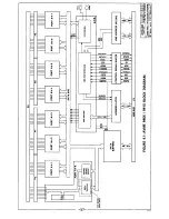
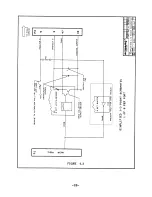
This chapter describes the circuitry of the Digital Board. A block diagram of this board is shown in Figure 4.1.
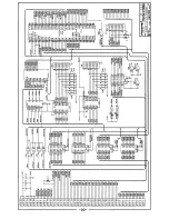
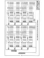
Schematics of the board are in chapter 7.
4.1 VMEbus Interface
The VMEbus Interface is composed of 3 functional areas:
•
Data Buffers (U27, U28)
•
Address Latch, Buffer and Comparators (U21, U3, U22, U24)
•
Control Buffers (U25, U26)
4.2 Board Controller
The Board Controller is composed of 5 functions: (U19)
•
Card and Register decoding
•
VMEbus Interface controller
•
PROM controller
•
Status register
•
Digital Port controller
4.3 Digital Port Section
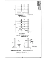
The Digital Port is composed of an output latch and an input buffer. A simplified I/O point schematic is shown in
figure 4.2.
- Output Latch (U1, U3, U5, U7, U9, U11, U13, U15)
- Input Buffer (Models AVME 946X only, U2, U4, U6, U8, U10, U12, U14, U16)


