1–28
Chapter 1: Nios II Hardware Development
Creating the Design Example
Nios II Hardware Development Tutorial
May 2011
Altera Corporation
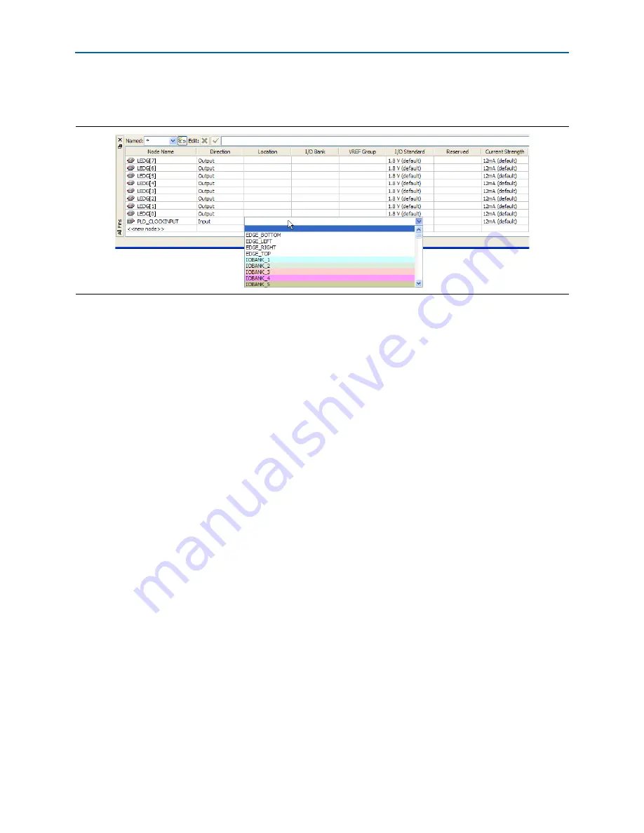
5. In the
PLD_CLOCKINPUT
row, double-click in the
Location
cell to access a list of
available pin locations.
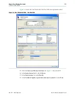
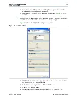
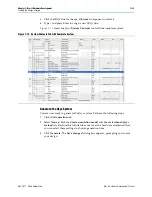
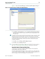
shows the GUI.
6. Select the appropriate FPGA pin that connects to the oscillator on the board.
1
If your design fails to work, recheck your board documentation for this step
first.
7. In the
PLD_CLOCKINPUT
row, double-click in the
I/O Standard
cell to access a
list of available I/O standards.
8. Select the appropriate I/O standard that connects to the oscillator on the board.
9. If you connected the LED pins in the board design schematic, repeat steps 4 to 8
for each of the LED output pins (
LEDG[0]
,
LEDG[1]
,
LEDG[2]
,
LEDG[3]
,
LEDG[4]
,
LEDG[5]
,
LEDG[6]
,
LEDG[7]
) to assign appropriate pin locations.
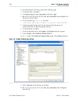
10. On the File menu, click
Close
to save the assignments.
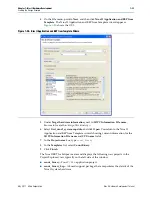
11. On the Assignments menu, click
Device
. The
Device
dialog box appears.
12. Click
Device and Pin Options
. The
Device and Pin Options
dialog box appears.
13. Click the
Unused Pins
page.
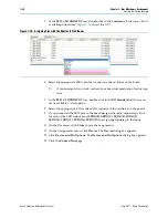
Figure 1–16. Assigning Pins with the Quartus II Pin Planner


