ATtiny22/22L
36
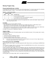
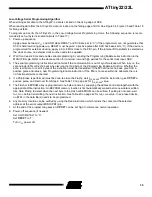
Figure 31. High-Voltage Serial Programming Waveforms
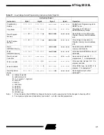
Table 14. High-Voltage Serial Programming Instruction Set
Instruction
Instruction Format
Operation Remarks
Instr.1
Instr.2
Instr.3
Instr.4
Chip Erase
PB0
PB1
PB2
0_1000_0000_00
0_0100_1100_00
x_xxxx_xxxx_xx
0_0000_0000_00
0_0110_0100_00
x_xxxx_xxxx_xx
0_0000_0000_00
0_0110_1100_00
x_xxxx_xxxx_xx
0_0000_0000_00
0_0100_1100_00
x_xxxx_xxxx_xx
Wait
t
WLWH_CE
after Instr.3 for the
Chip Erase cycle to finish.
Write Flash
High and Low
Address
PB0
PB1
PB2
0_0001_0000_00
0_0100_1100_00
x_xxxx_xxxx_xx
0_0000_00aa_00
0_0001_1100_00
x_xxxx_xxxx_xx
0_bbbb_bbbb_00
0_0000_1100_00
x_xxxx_xxxx_xx
Repeat Instr.2 for a new 256 byte
page. Repeat Instr.3 for each new
address.
Write Flash Low
byte
PB0
PB1
PB2
0_ i i i i_i i i i _00
0_0010_1100_00
x_xxxx_xxxx_xx
0_0000_0000_00
0_0110_0100_00
x_xxxx_xxxx_xx
0_0000_0000_00
0_0110_1100_00
0_0000_0000_00
Wait after Instr.3 until PB2 goes
high. Repeat Instr.1, Instr. 2 and
Instr.3 for each new address.
Write Flash
High byte
PB0
PB1
PB2
0_ i i i i_i i i i _00
0_0010_1100_00
x_xxxx_xxxx_xx
0_0000_0000_00
0_0111_0100_00
x_xxxx_xxxx_xx
0_0000_0000_00
0_0111_1100_00
0_0000_0000_00
Wait after Instr.3 until PB2 goes
high. Repeat Instr.1, Instr. 2 and
Instr.3 for each new address.
Read Flash
High and Low
Address
PB0
PB1
PB2
0_0000_0010_00
0_0100_1100_00
x_xxxx_xxxx_xx
0_0000_00aa_00
0_0001_1100_00
x_xxxx_xxxx_xx
0_bbbb_bbbb_00
0_0000_1100_00
x_xxxx_xxxx_xx
Repeat Instr.2 and Instr.3 for each
new address.
Read Flash
Low byte
PB0
PB1
PB2
0_0000_0000_00
0_0110_1000_00
x_xxxx_xxxx_xx
0_0000_0000_00
0_0110_1100_00
o_oooo_ooox_xx
Repeat Instr.1 and Instr.2 for each
new address.
Read Flash
High byte
PB0
PB1
PB2
0_0000_0000_00
0_0111_1000_00
x_xxxx_xxxx_xx
0_0000_0000_00
0_0111_1100_00
o_oooo_ooox_xx
Repeat Instr.1 and Instr.2 for each
new address.
Write EEPROM
Low Address
PB0
PB1
PB2
0_0001_0001_00
0_0100_1100_00
x_xxxx_xxxx_xx
0_0bbb_bbbb_00
0_0000_1100_00
x_xxxx_xxxx_xx
Repeat Instr.2 for each new
address.
Write EEPROM
byte
PB0
PB1
PB2
0_ i i i i_i i i i _00
0_0010_1100_00
x_xxxx_xxxx_xx
0_0000_0000_00
0_0110_0100_00
x_xxxx_xxxx_xx
0_0000_0000_00
0_0110_1100_00
0_0000_0000_00
Wait after Instr.3 until PB2 goes
high
Read EEPROM
Low Address
PB0
PB1
PB2
0_0000_0011_00
0_0100_1100_00
x_xxxx_xxxx_xx
0_0bbb_bbbb_00
0_0000_1100_00
x_xxxx_xxxx_xx
Repeat Instr.2 for each new
address.
MSB
MSB
MSB
LSB
LSB
LSB
0
1
2
3
4
5
6
7
8
9
10
SERIAL DATA INPUT
PB0
SERIAL INSTR. INPUT
PB1
SERIAL DATA OUTPUT
PB2
SERIAL CLOCK INPUT
XTAL1/PB3


