VERSION 1.9
J120 (38198-X)
MCU
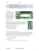
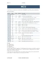
The J90 features an on-board micro controller (MCU: STM32F042F6P6) with 32 kByte Flash and 6kByte RAM.
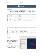
MCU pin description
Pin types:
PP - push/pull output
OD - open drain output
Ain - analog input
AF - alternate function
The power supply to the MCU is supplied by a 3.3V LDO regulator which is always on. So the MCU is powered as
soon as power is applied to the power input on J13. This allows the MCU to manage whether power should be
applied to the carrier board (with pin 7).
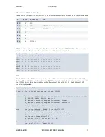
The MCU tunnels the console UART interface to the TX1/TX2. Some instructions are intercepted by the MCU
and executed by it. These instructions are not forwarded to the TX1/TX2.
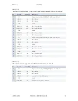
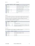
MCU Pin
Name
Type
Function
Description
1
PB8/BOOT0
-
-
10k pull down
2
PF0
OD
POWER
1: inactive, 0: press power button
3
PF1
PP
RESET
1: press reset button (10k pull down), 0: inactive
4
NRST
-
-
hardware power on reset of MCU (RC circuit)
5
VddA
-
-
analog 3.3V supply (by always on LDO)
6
PA0
Ain0
V12_IN
measure input voltage (voltage divider: 100k up/10k down)
7
PA1
PP
PWR_ON
1: enable power to J90 (10k pull down), 0: power off
8
PA2
AF
UART0_RX
UART 0 to TX1/TX2
9
PA3
AF
UART0_TX
UART 0 to TX1/TX2
10
PA4
PP
LED
0: LED off, 1: LED on (default MCU heartbeat)
11
PA5
AIN5
V3.3_IN
measure 3.3V rail (voltage divider: 10k up/10k down)
12
PA6
AIN6
V5_IN
measure 5.0V rail (voltage divider: 10k up/10k down)
13
PA7
OD
SLEEP
0: press sleep button (R30 must be installed), 1: inactive
14
PB1
Ain9
V1.8_IN
measure 1.8V rail (direct connection)
15
GND
-
-
Ground
16
VddA
-
-
digital 3.3V supply (by always on LDO)
17
PA9/PA11
AF
UART_TX
UART_TX to J7 connector (pin 2)
18
PA10/PA12
AF
UART_RX
UART_RX to J7 connector (pin 3)
19
PA13
-
SWDIO
SWD programming interface (J7 pin 5)
20
PA14
-
SWCLK
SWD programming interface (J7 pin 4)
AUVIDEA GMBH
TECHNICAL REFERENCE MANUAL
24

