background image

VERSION 1.9

J120 (38198-X)

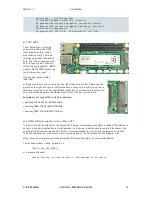
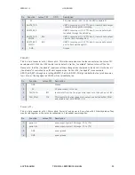
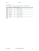
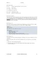
FAN (J8) 

This is a 4 pin connector with 1.25 mm pitch. This is the same pinout as the fan connector on the Jetson TX1 
development kit. With the J100 the fan is on by default. Use the „fan disable“ feature to turn off the fan. 

Please note, that the „fan disable“ requires a software change when compared to the dev kit. On the dev kit 
„fan disable“ is controlled by an I2C port expander line. On the J100 „fan disable“ is connected to 
GPIO19_AUD_RST (through an inverting MOSFET). Pull the GPIO19 (F2) high to disable the fan (pin 4 becomes 
low). A low or floating signal on GPIO19 will not disable the fan.


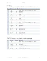
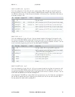
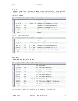
Power (J11) 

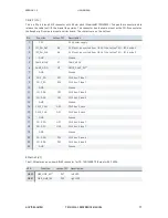
This is a 4 pin connector with 1.25 mm pitch. Power in 1 and power in 2 are or’ed with 2 Schottky diodes. They 
may be tied together or they may be connected to 2 redundant power supplies.  

Pin

Function

Jetson TX1

GPIO

Description

1

5V

-

-

5V power output (3.3V if only the MCU is powered)

2

UART0_TXD

-

-

UART 0 console port (3.3V TTL level): transmit data output 

- tunnelled through the watchdog 

3

UART0_RXD

-

-

UART 0 console port (3.3V TTL level): receive data input - 

tunnelled through the watchdog 

4

UART2_TXD 

SWCLK

B16

-

UART 2 console port (3.3V TTL level): transmit data output 

- port to flash watchdog MCU

5

UART2_RXD 

SWDIO

B15

-

UART 2 console port (3.3V TTL level): receive data output - 

port to flash watchdog MCU

6

GND

-

-

Ground

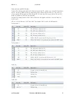
Pin

Function

Jetson TX1

Description

1

GND

-

Ground

2

5V

-

5V power supply to the fan

3

FAN_TACH

B17

tachometer from the fan (open drain input with 100k pull-up to 1.8V)

4

FAN_PWM

C16

PWM control to the fan (open drain output: controlled by FAN_PWM 

and „disable fan“ with GPIO19 - F2)

Pin

Function

Jetson TX1

Description

1

power in 1

-

power input: typical 12V (range: 7V to 17V)

2

power in 2

-

power input: typical 12V (range: 7V to 17V)

3

GND

-

power ground

4

GND

-

power ground

AUVIDEA GMBH

TECHNICAL REFERENCE MANUAL

 20

Summary of Contents for J120

Page 1: ...198 X J120 technical reference manual 38198 X Version 1 9 Preliminary March 2018 Auvidea GmbH Kellerberg 3 D 86920 Denklingen Tel 49 8243 7714 622 info auvidea com www auvidea com AUVIDEA GMBH TECHNICAL REFERENCE MANUAL 1 ...

Page 2: ... any of its contents may be reproduced copied modified or adapted without the prior written consent of the author unless otherwise indicated for stand alone materials You may share this document by any of the following means this PDF file may be distributed freely as long as no changes or modifications to the document are made For any other mode of sharing please contact the author at the email be...

Page 3: ...L 6 pin console access one I2S digital audio 6 pins each fan connector 4 pin mini HDMI out M 2 type M 2280 not operational on J120 rev 1 size 50 x 119 mm size of the PCB height 16 mm incl TX1 without heatsink without height of bottom side components of J100 height 21 mm incl TX1 without heatsink including height of bottom side components of J100 weight 42 grams just the J120 TX1 weight 144 grams T...

Page 4: ...ni standard mini USB 3 0 type A 2 4 2 micro USB 3 0 2 2 1 micro USB 2 0 OTG Wifi 2 antennas on TX1 module v 10 100 1000 Ethernet RJ45 1 1 1 2 TX1 i210 IMU MPU 9250 optional 9 axis sensor CAN controllers 1 1 1 1 SATA M 2 B 2242 standard standard 4x PCIe M 2 M 2280 PCIe slot M 2 2280 micro SD card SPI I2C 1 1 UART 1 2 2 2 2 CSI 2 22 pin 4 lanes 2 2 1 2 HDMI in 3 CSI 2 15 pin 2 lanes 2 2 I2S digital ...

Page 5: ... MOSFETs for controlled inrush ramp up with Lipo batteries four TX1 mount holes now connected to GND added LM75 temp sensor only one CAN bus and connector CAN2 to overcome problem with SPI1_CS0 line one CAN bus supported with TX1 firmware provided by Auvidea J120 Rev 4 38198 4 changed I2C pullup resistors from 1k to 10k to improve I2C signal low level J120 Rev 5 38198 5 I2S connector changed from ...

Page 6: ...VERSION 1 9 J120 38198 X J120 rev 5 top side J120 rev 5 bottom side AUVIDEA GMBH TECHNICAL REFERENCE MANUAL 6 ...

Page 7: ...nctions are tested HDMI out 1000BT Ethernet USB 3 0 on USB1 USB 2 0 on USB2 USB 3 mode requires modification of device tree file micro SD card power consumption with 12 V power supply Ubuntu booted and system idle Rev 3 and newer CSI 2 interface with B102 HDMI to CSI 2 module CAN bus communicating with Autoquad flight controller IMU with qtcreator test program M 2 2280 PCIe SSD Please have a look ...

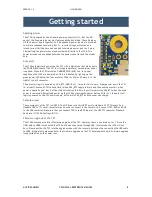
Page 8: ... 10 seconds This allows time for the Vdd_RTC supply to drain and the enable auto start when power is applied again Rev 2 of the J120 will shorten this time by actively draining Vdd_RTC when the main power is removed Alternatively power up the J120 by pressing the power button With rev 3 the auto start logic is powered by the 12V power supply not to drain Vdd_RTC and the super cap charge Console ac...

Page 9: ...tion up to 1080p60 This video then may be compressed or processed in the TX1 A typical application for this task is the GStreamer A driver developed by Ridgerun is provided and included in the Auvidea TX1 firmware Please contact us for the source code of the driver Toshiba 41M Pixel Camera Raytrix provides the C41 camera module Auvidea has developed a small interface board to connect the C41 camer...

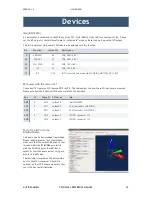
Page 10: ...ease make sure that the spidev3 0 device in dev is loaded Edit the RTIMUlibDemo ini file with the SPI settings for the IMU bus 3 select 0 Start the demo as root so it gets access to the SPI bus The IMU chip is located on the bottom side next to the JTAG connector The IMU is optional on the J120 Please make sure that your J120 has the IMU installed Pin Function Jetson TX1 Description 9 AD0 SDO E4 S...

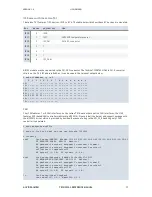
Page 11: ...he SPI_CS_0 handling only 1 CAN controller is populated sudo modprobe mcp251x sudo ip link set can0 up type can bitrate 1000000 ifconfig can0 Link encap UNSPEC HWaddr 00 00 00 00 00 00 00 00 00 00 00 00 00 00 00 00 UP RUNNING NOARP MTU 16 Metric 1 RX packets 0 errors 0 dropped 0 overruns 0 frame 0 TX packets 0 errors 0 dropped 0 overruns 0 carrier 0 collisions 0 txqueuelen 10 RX bytes 0 0 0 B TX b...

Page 12: ... type B SATA cards may fit mechanically but they will not work Please make sure that the M 2 card for the J120 has just one notch Examples of M 2 type M SSDs with PCIe interface Samsung 950 Pro 256GB MZ V5P256BW Samsung PM961 128GB MZVLW128HEGR Samsung SM951 512GB MZVPV512HDGL M 2 NVMe software support on the Jetson TX1 In order to use a M 2 key B SSD on the Jetson TX1 a kernel module supporting N...

Page 13: ...with 1 25 mm pitch Please check the website for details Figure 1 and 2 show the J120 rev 2 but the connector placement and pin numbering also applies to the J120 rev 1 Figure 1 connectors on the top side Figure 2 connectors on the bottom side AUVIDEA GMBH TECHNICAL REFERENCE MANUAL 13 ...

Page 14: ...ND Ground 8 USB3_TX2 E42 USB 3 0 transmit data 9 USB3_TX2 E41 USB 3 0 transmit data 10 5V 5V power controlled by USB1_EN_OC A18 max 900 mA 11 USB1 D A39 USB 2 0 data 12 USB1 D A38 USB 2 0 data 13 GND Ground 14 USB3_RX1 F44 USB 3 0 receive data 15 USB3_RX1 F43 USB 3 0 receive data 16 GND Ground 17 USB3_TX1 C44 USB 3 0 transmit data 18 USB3_TX1 C43 USB 3 0 transmit data Pin Function Jetson TX1 Descr...

Page 15: ...O F14 SPI1_MISO level shifted to 3 3V 14 SI F13 SPI1_MOSI level shifted to 3 3V 12 SCK G13 SPI1_CLK level shifted to 3 3V 22 CS E14 SPI1_CS0 level shifted to 3 3V 12 INT H3 GPIO20_AUD_INT low active with 10k pull up to 3 3V 17 RESET D7 GPIO5_CAM_FLASH_EN is inverted and connected to the RESET inputs Pin Function Jetson TX1 Description 15 SO F14 SPI1_MISO level shifted to 3 3V 14 SI F13 SPI1_MOSI l...

Page 16: ...VERSION 1 9 J120 38198 X 3 CAN1_L CAN data low 4 GND Ground 0V Function Jetson TX1 Description Pin AUVIDEA GMBH TECHNICAL REFERENCE MANUAL 16 ...

Page 17: ...Jetson TX1 I2C device 2 3 I2C_PM_CLK A6 3 3V level converted from 1 8V of the Jetson TX1 I2C device 2 4 GND Ground 5 CAM2_MCLK E7 CAM2_MCLK 6 CAM3_GPIO H7 GPIO3_CAM1_RST 7 GND Ground 8 CSI F_D1 E21 CSI 2 bus F lane 1 9 CSI F_D1 E20 CSI 2 bus F lane 1 10 GND Ground 11 CSI F D0 C23 CSI 2 bus F lane 0 12 CSI F D0 C22 CSI 2 bus F lane 0 13 GND Ground 14 CSI E_CLK G22 CSI 2 bus E clock 15 CSI E_CLK G21...

Page 18: ...7 HDMI data lane 1 7 GND Ground 8 DP1_TXD2 D37 HDMI data lane 0 9 DP1_TXD2 D36 HDMI data lane 0 10 GND Ground 11 DP1_TXD3 E36 HDMI clock 12 DP1_TXD3 E35 HDMI clock 13 GND Ground 14 CEC B33 HDMI_CEC 15 HDMI_DDC_SCL A35 DP1_AUX_CH 16 HDMI_DDC_SDA A34 DP1_AUX_CH 17 reserved not connected 18 PWR 5V power max 500 mA 19 HPD A33 inverted and connected to DP1_HPD Pin Function Jetson TX1 GPIO Description 1...

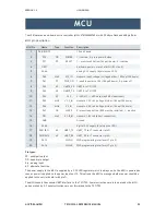
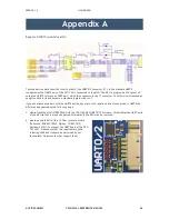
Page 19: ...r array To limit the power dissipation in the resistor array it is advised to sink or source a maximum current of 1 mA Pin 4 and 5 have the dual function to flash the watchdog MCU If the tunnelling of the UART0 port causes difficulties in a particular use case the J120 can be reconfigured so that the MCU is bypassed and a direct connection to the UART0 port of the TX1 and TX2 is provided Please ch...

Page 20: ...in Function Jetson TX1 GPIO Description 1 5V 5V power output 3 3V if only the MCU is powered 2 UART0_TXD UART 0 console port 3 3V TTL level transmit data output tunnelled through the watchdog 3 UART0_RXD UART 0 console port 3 3V TTL level receive data input tunnelled through the watchdog 4 UART2_TXD SWCLK B16 UART 2 console port 3 3V TTL level transmit data output port to flash watchdog MCU 5 UART...

Page 21: ...3V 6 GND Ground Pin Function Jetson TX1 GPIO Description 1 3 3V 3 3V power supply 2 I2S_MCLK F1 GPIO3_PBB 00 digital audio interface master clock 3 3V 3 I2S0_SIN G1 GPIO3_PB 01 digital audio interface 0 audio input 3 3V 4 I2S0_CLK G2 GPIO3_PB 03 digital audio interface 0 bit clock 3 3V 5 I2S0_LRCLK H1 GPIO3_PB 00 digital audio interface 0 word clock 3 3V 6 GND Ground Pin Function Jetson TX1 GPIO D...

Page 22: ...rface data 2 2 SD_DAT3 F18 SD card interface data 3 3 SD_CMD G19 SD card interface command 4 3 3V enabled by SDCARD_PWR_EN 1 H16 5 SD_CLK G18 SD card interface clock 6 GND Ground 7 SD_DAT0 H18 SD card interface data 0 8 SD_DAT1 H17 SD card interface data 1 9 SD_CD F17 GND Pin Function Jetson TX1 GPIO Description 1 Vdd_RTC A50 Realtime clock power input from backup battery or super cap Do not conne...

Page 23: ... 8V 1 8V power output 2 JTAG_AP_TRST_L B13 JTAG port of Jetson TX1 3 JTAG_AP_TCK B11 JTAG port of Jetson TX2 4 JTAG_AP_RTCK A14 JTAG port of Jetson TX3 5 JTAG_AP_TDO A13 JTAG port of Jetson TX4 6 JTAG_AP_TMS A12 JTAG port of Jetson TX5 7 NVJTAG_SEL A11 JTAG port of Jetson TX6 8 JTAG_AP_TDI B12 JTAG port of Jetson TX7 9 GND Ground AUVIDEA GMBH TECHNICAL REFERENCE MANUAL 23 ...

Page 24: ...1 PP RESET 1 press reset button 10k pull down 0 inactive 4 NRST hardware power on reset of MCU RC circuit 5 VddA analog 3 3V supply by always on LDO 6 PA0 Ain0 V12_IN measure input voltage voltage divider 100k up 10k down 7 PA1 PP PWR_ON 1 enable power to J90 10k pull down 0 power off 8 PA2 AF UART0_RX UART 0 to TX1 TX2 9 PA3 AF UART0_TX UART 0 to TX1 TX2 10 PA4 PP LED 0 LED off 1 LED on default M...

Page 25: ...CN2 header MCU firmware v1 1 This version of the MCU is limited to a UART baud rate of 38400 baud max Please set the TX1 TX2 to 38400 Please edit the file boot extlinux extlinux conf Please replace 115200n8 by 38400n8 TIMEOUT 30 DEFAULT primary MENU TITLE p2371 2180 eMMC boot options LABEL primary MENU LABEL primary kernel LINUX boot Image INITRD boot initrd FDT boot tegra210 jetson auvidea j90 dt...

Page 26: ...nce problems with the UART0 port and your use case requires a direct connection to UART0 the MCU may be bypassed by the following steps 1 please flash the MCU STM32F042 with the J90 J140 MCU UART OFF firmware This disables the UART ports of the MCU so that it may be bypassed Alternatively the MCU may be removed 2 please populate RN1 with a 10 Ohm resistor network Panasonic EXB 24V100JX Digikey Y51...

Page 27: ...VERSION 1 9 J120 38198 X FAQ 1 to be added AUVIDEA GMBH TECHNICAL REFERENCE MANUAL 27 ...

Page 28: ...al If you have found any typos or errors in this document please let us know This is the preliminary version of this data sheet Please treat all specifications with caution as there may be any typos or errors The Auvidea Team AUVIDEA GMBH TECHNICAL REFERENCE MANUAL 28 ...

Reviews: