3. Endian Settings for 16-bit Bus Width Connection
S1R72V17 CPU Connection Guide
EPSON 9
(Rev. 1.0)
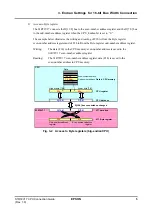
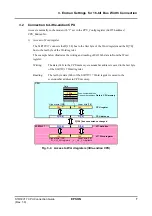
3) Access to FIFO register
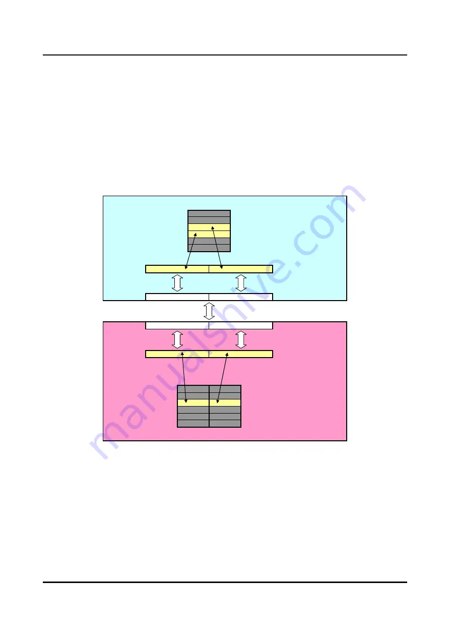
The S1R72V17 connects the D[7:0] bus to the even-number address register and the D[15:8] bus
to the odd-number address register when the CPU_Endian bit is set to “1.”
The example below illustrates transmission from the USB bus in the sequence C1h/C2h and
receiving in the sequence C1h/C2h.
Writing:
The data (C1h) in the CPU memory even-number address is sent from the USB
bus as the first data.
Reading:
The first data received from the USB bus (C1h) is saved to the even-number
address in CPU memory.
CPU
Data
・・・・
・・・・
C1h
Even-number address
C2h
Odd-number address
Data in CPU memory
・・・・
・・・・
Higher byte [15:8]
Lower byte [7:0]
C2h
C1h
CPU register
D[15:8]
D[7:0]
CPU data bus
D[15:0] bus connected unchanged
S1R72V17
D[15:8]
D[7:0]
V17 data bus
C2h
C1h
V17 Byte register
Odd-number address
Even-number address
register
register
Data[15:8]
Data[7:0]
・・・・
・・・・
V17 FIFO data
・・・・
・・・・
(2) C2h
(1) C1h
Sent via USB bus in order (1), (2).
(4)
・・・・
(3)
・・・・
・・・・
・・・・
・・・・
・・・・
Fig. 3-6 Access to FIFO registers (little-endian CPU)


