background image

37

Figure 2.10 shows the object code format of the EEPROM write instruction.

op

15

8

7

0

op

Legend:
op:  Operation field

EEPMOV

Figure 2.10   EEPROM Write Instruction Object Code Format

2.6

Operating States

2.6.1

Overview

The CPU operates in three states: the program execution state, exception-handling state, and
power-down state. Figure 2.11 summarizes these states. Figure 2.12 shows the state transitions.

Chip state 

Program execution state

CPU executes program

Exception-handling state

Transitory state that changes CPU execution flow 
at a reset or interrupt

Power-down state

CPU halts to conserve power

Sleep mode

Figure 2.11   Operating States

Summary of Contents for H8/3152

Page 1: ...Hitachi Single Chip Microcomputer H8 3150 Series H8 3152 HD6483152 H8 3153 HD6483153 H8 3155 HD6483155 H8 3156 HD6483156 H8 3158 HD6483158 Hardware Manual ADE 602 182 Rev 1 0 3 11 99 Hitachi Ltd ...

Page 2: ...of bodily injury such as aerospace aeronautics nuclear power combustion control transportation traffic safety equipment or medical equipment for life support 4 Design your application so that the product is used within the ranges guaranteed by Hitachi particularly for maximum rating operating supply voltage range heat radiation characteristics installation conditions and other characteristics Hita...

Page 3: ...d a watchdog timer WDT On chip EEPROM makes the H8 3150 series ideal for applications requiring nonvolatile data storage including smart cards and portable data banks Security functions protect data in the internal memory against illegal external reading and writing This manual describes the H8 3150 series hardware For details of the instruction set refer to the H8 300 Series Programming Manual ...

Page 4: ... 3 2 Memory Data Formats 16 2 4 Addressing Modes 17 2 4 1 Addressing Modes 17 2 4 2 Effective Address Calculation 19 2 5 Instruction Set 22 2 5 1 Data Transfer Instructions 24 2 5 2 Arithmetic Operations 26 2 5 3 Logic Operations 27 2 5 4 Shift Operations 27 2 5 5 Bit Manipulations 29 2 5 6 Branching Instructions 33 2 5 7 System Control Instructions 35 2 5 8 EEPROM Write Instruction 36 2 6 Operati...

Page 5: ...ction 5 Watchdog Timer WDT 57 5 1 Overview 57 5 1 1 Features 57 5 1 2 Block Diagram 58 5 1 3 Register Configuration 58 5 1 4 Vector Configuration 59 5 2 Register Descriptions 59 5 2 1 Timer Counter TCNT 59 5 2 2 Timer Control Status Register TCSR 60 5 2 3 Timer Counter Write Address TCWA 61 5 3 Operation 63 5 3 1 Checking Application Program Execution Area 63 5 3 2 Checking the Procedure for Writi...

Page 6: ...edure 89 8 5 3 Reading the Protect Bits 91 8 6 Notes on Usage 92 8 7 Notes on Usage of H8 3153 94 Section 9 I O Ports 97 9 1 Overview 97 9 1 1 Block Diagram 97 9 1 2 Register Configuration 99 9 2 Register Descriptions 99 9 2 1 Data Register DR 99 9 2 2 Data Direction Register DDR 100 9 3 Pin Functions 100 Section 10 Clock Pulse Generator 103 10 1 Overview 103 10 2 System Control Register 104 Secti...

Page 7: ...nal clock frequency 114 12 2 6 AC Characteristics 3 V CPU operates at half of the external clock frequency 115 12 2 7 DC Characteristics 3 V CPU operates at the external clock frequency 116 12 2 8 AC Characteristics 3 V CPU operates at the external clock frequency 117 Appendix A Instruction Set 119 Appendix B Operation Code Map 127 Appendix C Register Field 129 C 1 Register Field 1 129 C 2 Registe...

Page 8: ...tures of the H8 3150 series Table 1 1 Features Item Specification CPU H8 300 CPU Two way general register configuration Sixteen 8 bit registers or Eight 16 bit registers High speed operation Maximum clock rate internal clock 5 MHz at 5 V Add subtract 0 4 µs Multiply divide 2 8 µs Streamlined concise instruction set Instruction length 2 or 4 bytes Register register arithmetic and logic operations M...

Page 9: ...ccidental writing and erasing On chip voltage pumping circuit Built in oscillator and timer Write erase time max 10 ms rewrite 5 ms erase overwrite Rewrite endurance 105 times Data retention time 10 years ROM H8 3152 24 kbytes H8 3153 32 kbytes H8 3155 16 kbytes H8 3156 16 kbytes H8 3158 46 kbytes RAM H8 3152 512 bytes H8 3153 1 kbyte H8 3155 512 bytes H8 3156 512 bytes H8 3158 1 kbyte I O ports T...

Page 10: ...O input ports before executing a SLEEP instruction When writing to the DDR7 and DDR6 bits use the MOV instruction instead of the bit manipulation instruction Power Single voltage power supply 4 5 V to 5 5 V 2 7 V to 3 3 V Clock frequency range When the CPU operates at the external clock frequency CPUCS0 1 fCLK 1 MHz to 5 MHz VCC 4 5 V to 5 5 V fCLK 1 MHz to 4 MHz VCC 2 7 V to 3 3 V When the CPU op...

Page 11: ...1 shows an internal block diagram of the H8 3150 series H8 300 CPU System control logic ROM RAM EEPROM RNG I O port WDT I O 1 IRQ I O 2 IRQ Data bus Address bus Clock divider VCC VSS CLK RES Security logic Figure 1 1 Block Diagram ...

Page 12: ...t Figure 1 2 shows the standard COT chip on tape pattern of the H8 3150 series Figure 1 3 shows the bonding pad arrangement of the wafer product The COT is mounted on a tape VCC RES CLK NC VSS NC I O 1 IRQ NC Figure 1 2 Standard COT Pattern Electrode Surface ...

Page 13: ...Q CLK VCC RES User PAD Note This figure shows the relative locations of the bonding pads on the chip For accurate locations and chip dimensions refer to the separately supplied specifications Figure 1 3 Bonding Pad Arrangement ...

Page 14: ... this port can receive interrupt input I O 2 IRQ 2 I O I O port 2 One bit data input output port Software can select input or output Interrupt In sleep mode this port can receive interrupt input Notes 1 An input pull up MOS is connected to the RES pin as shown in figure 1 4 Input pull up MOS Input buffer Internal RES signal VCC RES pin Figure 1 4 Block Diagram of RES Pin 2 The I O 1 IRQ and I O 2 ...

Page 15: ...w Two way register configuration Sixteen 8 bit general registers or Eight 16 bit general registers Instruction set with 55 basic instructions including Multiply and divide instructions Powerful bit manipulation instructions EEPROM write instruction Eight addressing modes Register direct Rn Register indirect Rn Register indirect with displacement d 16 Rn Register indirect with post increment or pre...

Page 16: ... instruction is executed in two to four states Maximum clock rate is 5 MHz internal clock at 5 V 8 or 16 bit register register add or subtract 0 4 µs 8 8 bit multiply 2 8 µs 16 8 bit divide 2 8 µs Power down states Entered by the SLEEP instruction ...

Page 17: ... 5 4 3 2 1 0 I U H U N Z V C CCR PC SP 0 7 0 7 R0H R1H R2H R3H R4H R5H R6H R7H R0L R1L R2L R3L R4L R5L R6L R7L General registers Rn Control registers CR 15 0 Legend SP PC CCR I U H N Z V C Stack pointer Program counter Condition code register Interrupt mask bit User bit Half carry flag Negative flag Zero flag Overflow flag Carry flag Figure 2 1 CPU Registers ...

Page 18: ...write instruction is executed R7 also functions as the stack pointer used implicitly by hardware in exception handling and subroutine calls In assembly language coding R7 can also be denoted by the symbol SP As indicated in figure 2 2 SP R7 points to the top of the stack SP R7 Free area Stack area Figure 2 2 Stack Pointer 2 2 2 Control Registers The CPU control registers include a 16 bit program c...

Page 19: ...nd read by software for its own purposes using the LDC STC ANDC ORC and XORC instructions Bit 3 Negative Flag N Indicates the most significant bit sign bit of data Bit 2 Zero Flag Z Set to 1 to indicate zero data and cleared to 0 to indicate non zero data Bit 1 Overflow Flag V Set to 1 when an arithmetic overflow occurs and cleared to 0 at other times Bit 0 Carry Flag C Set to 1 when a carry occur...

Page 20: ...cuted after a reset 2 3 Data Formats The H8 300 CPU can process 1 bit data 4 bit BCD data 8 bit byte data and 16 bit word data Bit manipulation instructions operate on 1 bit data specified as bit n n 0 1 2 7 in a byte operand All arithmetic instructions except ADDS and SUBS can operate on byte data The MOV W ADD W SUB W CMP W ADDS SUBS MULXU 8 bits 8 bits and DIVXU 16 bits 8 bits instructions oper...

Page 21: ...Don t care MSB LSB 7 0 MSB LSB 15 0 7 4 3 0 7 4 3 0 Don t care Don t care Lower digit Upper digit Upper digit Lower digit RnH RnL RnH RnL Rn RnH RnL Register no Data type Data format 1 bit data 1 bit data Byte data Byte data Word data 4 bit BCD data 4 bit BCD data Legend RnH General register high byte RnL General register low byte MSB Most significant bit LSB Least significant bit Figure 2 3 Regis...

Page 22: ...4 3 2 1 0 7 0 MSB LSB MSB LSB MSB LSB MSB LSB MSB LSB Upper 8 bits Lower 8 bits CCR CCR Address Data type Data format Address n Address n Even address Odd address Even address Odd address Even address Odd address 1 bit data Byte data Word data Byte data CCR on stack Word data on stack Legend CCR Condition code register Note Ignored on return Figure 2 4 Memory Data Formats When the stack is accesse...

Page 23: ...rect aa 8 1 Register Direct Rn The register field of the instruction specifies an 8 or 16 bit general register containing the operand Only the MOV W ADD W SUB W CMP W ADDS SUBS MULXU 8 bits 8 bits and DIVXU 16 bits 8 bits instructions have 16 bit operands 2 Register Indirect Rn The register field of the instruction specifies a 16 bit general register containing the address of the operand 3 Registe...

Page 24: ...ress of the operand in memory The absolute address may be 8 bits long aa 8 or 16 bits long aa 16 The MOV B and bit manipulation instructions can use 8 bit absolute addresses The MOV B MOV W JMP and JSR instructions can use 16 bit absolute addresses For an 8 bit absolute address the upper 8 bits are assumed to be 1 H FF The address range is H FF00 to H FFFF 65280 to 65535 6 Immediate xx 8 or xx 16 ...

Page 25: ...ed at the address preceding the specified address See section 2 3 2 Memory Data Formats for further information 2 4 2 Effective Address Calculation Table 2 2 shows how effective addresses are calculated in each of the addressing modes Arithmetic and logic instructions use register direct addressing 1 The ADD B ADDX SUBX CMP B AND OR and XOR instructions can also use immediate addressing 6 Data tra...

Page 26: ...t register contents op reg 0 3 4 6 7 15 0 15 0 15 Register indirect 3 0 15 op disp reg 0 3 4 6 7 15 16 bit register contents 16 bit register contents 0 15 Register indirect with displacement d 16 Rn 4 0 15 op reg 0 3 4 6 7 15 16 bit register contents 0 15 1 or 2 Register indirect with post increment Rn 0 15 op reg 0 3 4 6 7 15 16 bit register contents 0 15 1 or 2 1 for a byte operand 2 for a word ...

Page 27: ...dress aa 16 6 op IMM 0 7 8 15 Immediate xx 8 Operand is 1 byte immediate data IMM op 0 15 Immediate xx 16 Operand is 2 byte immediate data 7 0 15 PC contents disp Sign extension 0 15 op disp 0 7 8 15 PC relative d 8 PC 8 op abs 16 bit memory contents H 00 0 7 8 15 0 15 8 7 0 15 Memory indirect aa 8 Legend reg regm regn General registers op Operation field disp Displacement IMM Immediate data abs A...

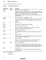
Page 28: ... 1 Arithmetic operations ADD SUB ADDX SUBX INC DEC ADDS SUBS DAA DAS MULXU DIVXU CMP NEG 14 Logic operations AND OR XOR NOT 4 Shift SHAL SHAR SHLL SHLR ROTL ROTR ROTXL ROTXR 8 Bit manipulation BSET BCLR BNOT BTST BAND BIAND BOR BIOR BXOR BIXOR BLD BILD BST BIST 14 Branch Bcc 2 JMP BSR JSR RTS 5 System control SLEEP LDC STC ANDC ORC XORC NOP RTE 8 EEPROM write EEPMOV 1 Total 55 Notes 1 POP Rn is id...

Page 29: ...estination Rs General register source Rn General register EAd Destination operand EAs Source operand CCR Condition code register N N negative bit of CCR Z Z zero bit of CCR V V overflow bit of CCR C C carry bit of CCR PC Program counter SP Stack pointer IMM Immediate data disp Displacement Addition Subtraction Multiplication Division AND logical OR logical Exclusive OR logical Move Not 3 8 16 3 8 ...

Page 30: ... or moves immediate data to a general register The Rn Rn d 16 Rn aa 16 xx 16 Rn and Rn addressing modes are available for byte or word data The xx 8 and aa 8 addressing modes are available for byte data only Specify word size operands for R7 and R7 POP W SP Rn Pops a 16 bit general register from the stack Identical to MOV W SP Rn PUSH W Rn SP Pushes a 16 bit general register onto the stack Identic...

Page 31: ... rm xx16 Rn POP PUSH xx8 Rn 15 8 7 0 abs rn op 15 8 7 0 IMM rn op aa 8 Rn Rm Rn Rn Rm Rm Rn 15 8 7 0 op disp rn rm d 16 Rm Rn Rm Rn MOV 15 8 7 0 op IMM rn 15 8 7 0 op abs rn aa 16 Rn Legend op Operation field rm rn Register field disp Displacement abs Absolute address IMM Immediate data Figure 2 5 Data Transfer Instruction Object Code Formats ...

Page 32: ...ents a general register ADDS SUBS W Rd 1 Rd Rd 2 Rd Adds or subtracts immediate data to or from data in a general register The immediate data must be 1 or 2 DAA DAS B Rd decimal adjust Rd Decimal adjusts 4 bit BCD data in a general register by referring to CCR MULXU B Rd Rs Rd Performs 8 bit 8 bit unsigned multiplication on data in two general registers providing a 16 bit result DIVXU B Rd Rs Rd P...

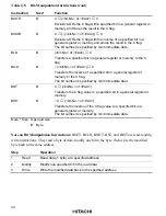
Page 33: ... on a general register and another general register or immediate data NOT B Rd Rd Obtains the one s complement logical complement of general register contents Note Size Operand size B Byte 2 5 4 Shift Operations Table 2 7 describes the shift instructions Table 2 7 Shift Instructions Instruction Size Function SHAL SHAR B Rd shift Rd Performs an arithmetic shift operation on general register content...

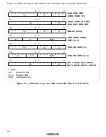
Page 34: ... op IMM 15 8 7 0 op rn rm 15 8 7 0 15 8 7 0 op rn rm 15 8 7 0 op rn 15 8 7 0 op rn rm IMM rn op rn AND OR XOR xx 8 AND OR XOR Rm ADD ADDX SUBX CMP xx 8 MULXU DIVXU ADDS SUBS INC DEC DAA DAS NEG NOT ADD SUB CMP ADDX SUBX Rm Legend op Operation field rm rn Register field IMM Immediate data Figure 2 6 Arithmetic Logic and Shift Instruction Object Code Formats ...

Page 35: ...BTST B bit No of EAd Z Tests a specified bit in a general register or memory and sets or clears the Z flag accordingly The bit number is specified by 3 bit immediate data or the lower three bits of a general register BAND B C bit No of EAd C ANDs the C flag with a specified bit in a general register or memory and stores the result in the C flag BIAND B C bit No of EAd C ANDs the C flag with the in...

Page 36: ... in a general register or memory to the C flag The bit number is specified by 3 bit immediate data BST B C bit No of EAd Transfers the C flag value to a specified bit in a general register or memory BIST B C bit No of EAd Transfers the inverse of the C flag value to a specified bit in a general register or memory The bit number is specified by 3 bit immediate data Note Size Operand size B Byte Not...

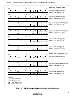
Page 37: ...0 op op IMM 0 0 0 0 Operand register indirect Rn Bit No immediate xx 3 Operand register direct Rn Bit No immediate xx 3 BAND BOR BXOR BLD BST Operand absolute aa 8 Bit No register direct Rm Operand absolute aa 8 Bit No immediate xx 3 Operand register indirect Rn Bit No register direct Rm Operand register indirect Rn Bit No immediate xx 3 Operand register direct Rn Bit No immediate xx 3 Operand reg...

Page 38: ... 0 0 0 0 0 op op IMM 0 0 0 0 Operand register indirect Rn Bit No immediate xx 3 Operand register direct Rn Bit No immediate xx 3 BIAND BIOR BIXOR BILD BIST Legend op Operation field rm rn Register field abs Absolute address IMM Immediate data Figure 2 7 Bit Manipulation Instruction Object Code Formats cont ...

Page 39: ... Never false Never BHI High C Z 0 BLS Low or same C Z 1 BCC BHS Carry clear high or same C 0 BCS BLO Carry set low C 1 BNE Not equal Z 0 BEQ Equal Z 1 BVC Overflow clear V 0 BVS Overflow set V 1 BPL Plus N 0 BMI Minus N 1 BGE Greater or equal N V 0 BLT Less than N V 1 BGT Greater than Z N V 0 BLE Less or equal Z N V 1 JMP Branches unconditionally to a specified address BSR Branches to a subroutine...

Page 40: ... JSR aa 16 JSR aa 8 RTS op disp cc rm op abs 15 8 7 0 op 15 8 7 0 15 8 7 0 15 8 7 0 abs op abs 15 8 7 0 op disp 15 8 7 0 op 0 0 0 0 rm 15 8 7 0 op abs 15 8 7 0 op 15 8 7 0 Legend op Operation field cc Condition field rm Register field disp Displacement abs Absolute address Figure 2 8 Branching Instruction Object Code Formats ...

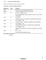
Page 41: ...mediate data or general register contents to the condition code register STC B CCR Rd Copies the condition code register to a specified general register ANDC B CCR IMM CCR Logically ANDs the condition code register with immediate data ORC B CCR IMM CCR Logically ORs the condition code register with immediate data XORC B CCR IMM CCR Logically exclusive ORs the condition code register with immediate...

Page 42: ... Instruction Table 2 11 describes the EEPROM write instruction Table 2 11 EEPROM Write Instruction Instruction Size Function EEPMOV If R4L 0 then repeat R5 R6 R4L 1 R4L until R4L 0 else next Transfers a data block to EEPROM according to parameters set in general registers R4L R5 and R6 R4L size of block bytes R5 starting source address R6 starting destination address Execution of the next instruct...

Page 43: ...e CPU operates in three states the program execution state exception handling state and power down state Figure 2 11 summarizes these states Figure 2 12 shows the state transitions Chip state Program execution state CPU executes program Exception handling state Transitory state that changes CPU execution flow at a reset or interrupt Power down state CPU halts to conserve power Sleep mode Figure 2 ...

Page 44: ...ion handling the stack pointer is referenced and the program counter and condition code register are saved 2 6 4 Power Down State The power down state consists of a sleep mode Sleep mode is entered from the program execution state when the SLEEP instruction is executed Operation of the CPU clocks and all other on chip peripheral modules is halted The on chip peripheral modules enter the reset stat...

Page 45: ... instruction execution is completed Cannot be masked EWE Interrupt signal level is detected Interrupt exception handling starts when the execution of the instruction following the EWE write instruction is executed Cannot be masked Low External interrupt IRQ Falling edge is detected Interrupt exception handling starts immediately when an falling edge is detected on the I O 1 IRQ or I O 2 IRQ pin in...

Page 46: ...l interrupts UDF and EWE interrupts of WDT In sleep mode only the I O 1 IRQ and I O 2 IRQ pins function as interrupt pins and are capable of input The IRQ interrupt uses falling edge detection and an interrupt request is accepted if the I bit in CCR is cleared to 0 See section 9 I O Ports for I O 1 IRQ and I O 2 IRQ specification details and section 5 Watchdog Timer for UDF and EWE interrupt detai...

Page 47: ... of the first instruction that will be executed after the return 2 Registers must be saved and restored by word access starting at an even address Ignored on return Save on stack Even address Figure 2 13 Stack before and after Interrupt Exception Handling Sequence 2 7 4 Reset Start Timing The reset start timing of the H8 3150 series that is the number of clock cycles between the rising edge of RES...

Page 48: ...ails on tcyc see figures 12 1 and 12 5 in section 12 Electrical Characteristics 2 8 2 Transition to Sleep Mode Sleep mode is entered by executing the SLEEP instruction In sleep mode the CPU clock and on chip functions halt reducing power dissipation As long as the necessary voltage is supplied however the contents of CPU registers RNG registers WDT registers RAM and I O port registers DR and DDR a...

Page 49: ... IRQ pins can receive interrupt signals When a high to low transition occurs in the input the external clock is supplied to the CPU and on chip modules sleep mode is cleared and interrupt exception handling starts The external clock must be stable when the interrupt signal goes low Figure 2 15 shows the transition sequence from sleep mode to interrupt handling Figure 2 16 shows the timing of an in...

Page 50: ...Sleep Mode Note The RES I O 1 IRQ and I O 2 IRQ signals must be held high during sleep mode Sleep mode CLK CCR I bit CLK 0 MHz to tcyc I O 1 IRQ or I O 2 IRQ State IRQ Operating state Power down state Operating state CCR I bit cleared to 0 Interrupt exception handling SLEEP instruction Figure 2 16 Interrupt Timing in Sleep Mode ...

Page 51: ...EWE interrupt UDF interrupt H 000A H 000B H 000C H 000D TCSR TCNT Registers for WDT H FFFC H FFFD RCSR RNRR TCWA SYSCR Registers for RNG Register for WDT H FFF0 H FFF2 H FFF3 H FFF4 H FFF5 Address Address Access Reset PBM 1 PBM 0 EEPROM data area 8 kbytes EEPROM protection area Read only Read only Read only Word Byte x x x x x x x Access possible Access not possible x Note Switched by EPR PBM bit ...

Page 52: ...B H 000C H 000D TCSR TCNT Registers for WDT H FFFC H FFFD RCSR RNRR TCWA SYSCR Registers for RNG Register for WDT H FFF0 H FFF2 H FFF3 H FFF4 H FFF5 Address Address Access Reset PBM 1 PBM 0 EEPROM data area 16 kbytes EEPROM protection area Read only Read only Read only Word Byte x x x x x x x Access possible Access not possible x Note Switched by EPR PBM bit Register for CPU clock selection 512 by...

Page 53: ...ddress Address Access Reset PBM 1 PBM 0 EEPROM data area 1 kbyte EEPROM protection area Read only Read only Read only Word Byte x x x x x x x x x Access possible Access not possible x Switched by EPR PBM bit Register for CPU clock selection 128 bytes Note Shaded areas are unavailable to the user User programs must not access these areas TCSR TCNT Registers for WDT H FFFC H FFFD RCSR RNRR TCWA Regi...

Page 54: ...y Read only Word Byte x x x x x x x x x Access possible Access not possible x Switched by EPR PBM bit 128 bytes Note Shaded areas are unavailable to the user User programs must not access these areas H FFF8 ECR EPR DR DDR H FFF9 H FFFE H FFFF Registers for I O port Registers for EEPROM SYSCR H FFF3 H FFF4 Register for CPU clock selection TCSR TCNT Registers for WDT H FFFC H FFFD RCSR RNRR TCWA Reg...

Page 55: ...B H 000C H 000D TCSR TCNT Registers for WDT H FFFC H FFFD RCSR RNRR TCWA SYSCR Registers for RNG Register for WDT H FFF0 H FFF2 H FFF3 H FFF4 H FFF5 Address Address Access Reset PBM 1 PBM 0 EEPROM data area 16 kbytes EEPROM protection area Read only Read only Read only Word Byte x x x x x x x Access possible Access not possible x Note Switched by EPR PBM bit Register for CPU clock selection 512 by...

Page 56: ...gh speed random number generation Generates a 16 bit random number in 3 2 ms typical value Generation time does not depend on external clocks Continuous random number generation Generates a new random number automatically when the register that holds a random number is read 4 1 2 Register Configuration Table 4 1 shows the RNG registers Table 4 1 RNG Registers Name Abbreviation R W Initial Value Ad...

Page 57: ...o 0 and the RRDY bit holds the value Writing 1 to the GE bit starts random number generation in the RNG and when the generated random number is written to RNRR the RRDY bit is set to 1 Reading RNRR while the RNG is active GE 1 starts generating and writing a new random number to RNRR therefore the RRDY bit is cleared to 0 Bit 7 RRDY Description 0 Clearing condition When 0 is written to the GE bit ...

Page 58: ... these bits 4 2 2 RNG Result Register RNRR RNRR is a 16 bit read only register and cannot be written to RNRR must always be read in word size The initial value is undefined The random number generated in the RNG is written to RNRR Reading RNRR while the RNG is active GE 1 clears the RRDY to 0 then automatically generates and writes a new random number to RNRR Bit 15 14 13 12 11 10 9 8 7 6 5 4 3 2 ...

Page 59: ... End Figure 4 1 Random Data Writing Procedure Using RNG To generate a random number first write 1 to the GE bit to start the RNG When a random number is generated the 16 bit random number is written to RNRR and the RRDY bit is set to 1 Reading the random number from RNRR in this state clears the RRDY bit to 0 and a new 16 bit random number is generated and written to RNRR Repeat these steps until ...

Page 60: ...r generation for this program is shown in table 4 2 Table 4 2 Random Number Generation Performance reference values Data Length Perfor mance 16 Bits 80 Bits 128 Bits 160 Bits 192 Bits 256 Bits 288 Bits 384 Bits 512 Bits Execution time 3 2 ms 16 ms 26 ms 32 ms 39 ms 53 ms 58 ms 77 ms 103 ms 4 4 Notes on Usage 1 Check that the RRDY bit is 1 before reading the data from RNRR If read while the RRDY bi...

Page 61: ...outine can monitor the instructions in the area pointed to by the PC that is saved in the stack area to check whether an EEPMOV instruction will be executed in the correct procedure and with the correct data UDF and EWE interrupts are not masked by the I bit setting in the CCR Setting the halt flag after the above checking is completed stops all the on chip functions To exit from this state and en...

Page 62: ...controller TCNT Timer counter TCSR Timer control status register TCWA Timer control write address Figure 5 1 WDT Block Diagram 5 1 3 Register Configuration Table 5 1 lists the WDT registers Table 5 1 WDT Registers Name Abbr R W Initial Value Address Timer counter write address TCWA R W H FF H FFF5 Timer control status register TCSR R W H 2C H FFFC Timer counter TCNT R W H FF H FFFD Note Only 1 can...

Page 63: ... SYSCR is 1 a TCNT underflow H 00 H FF occurs When TCSR is written to after reset TCNT starts decrementing the value by counting pulses of the internal clock selected by the CS1 and CS0 bits in TCSR The number of clock cycles before TCNT underflows depends on the CS1 and CS0 bit settings When a TCNT underflow occurs the UDF bit in TCSR is set to 1 then a UDF interrupt is issued TCNT starts decreme...

Page 64: ...y a low level input to the RES pin Bit 7 6 5 4 3 2 1 0 UDF EWE HLT CS1 CS0 Initial value 0 0 1 0 1 1 0 0 Read Write R R W R R W R R R W R W Note Only 1 can be written to bit 6 to set the flag Bit 7 Underflow Flag UDF Indicates that a UDF interrupt was issued due to TCNT underflow H 00 H FF Bit 7 UDF Description 0 Clearing condition When RTE instruction is executed while UDF 1 Initial value 1 Setti...

Page 65: ...Although not used at present the reserved bits may be used in the future When writing to TCSR write 0 into bits 3 and 2 Bits 1 and 0 Clock Select 1 and 0 CS1 and CS0 Select one from four clock sources obtained by dividing the CLK pin input as the input to TCNT Bit 1 CS1 Bit 0 CS0 Description 0 0 CLK 32 Initial value 1 CLK 64 1 0 CLK 128 1 CLK 256 5 2 3 Timer Counter Write Address TCWA TCWA has fou...

Page 66: ...an be specified as an operand write data of the write instruction for reloading TCNT the initially written value is always reloaded to TCNT Bits 3 to 1 Reserved Always read as 1 and cannot be written to Bit 0 Write Address Disable WAD Enables or disables TCWA When WAD 1 TCWA does not operate When writing data to IA15 to IA12 in TCWA set the WAD bit to 0 at the same time the TCWA data becomes valid...

Page 67: ...ternal IRQ pin inputs The WDT sets the HLT bit to 1 when the counter value underflows again between the UDF interrupt acceptance and RTE instruction completion The WDT sets the HLT bit to 1 also when 1 is written to the EWE bit between the UDF interrupt acceptance and RTE instruction completion Figure 5 4 shows an example of checking the application execution area by using the UDF interrupt routin...

Page 68: ...BTST 7 TCSR reconfirmation BEQ ERROR MOV W 2 SP R0 MOV W H 1000 R1 MOV W H 1FFF R2 CMP W R0 R1 if H 1000 PC H 1FFF then PASS BHS ERROR CMP W R0 R2 BLO ERROR RTE ERROR MOV B H FF R0L MOV B R0L TCSR system halt End H 1000 MOV UDF interrupt ADD Application program area 2 H 1FFF SP SP 1 SP 2 SP 3 CCR CCR PCH 1 PCL 1 Stack area PC marked with 1 points to address marked with 2 Figure 5 4 Memory Contents...

Page 69: ...RQ requests include external IRQ pin inputs When a TCNT underflow and a write to EWE occur at the same time an exception by the EWE interrupt is processed then an exception by the TCNT underflow is processed The WDT sets the UDF bit to 1 and issues a UDF interrupt when the counter value underflows in the EWE interrupt routine The WDT sets the HLT bit is set to 1 when 1 is written to the EWE bit ag...

Page 70: ...n be notified of the abnormal operation by outputting a signal to an I O pin Example of program in EWE interrupt routine EWEentry BTST 6 TCSR reconfirmation BEQ ERROR MOV W 2 SP R0 MOV W H 7B5C R1 MOV W H 598F R2 MOV W R0 R3 CMP W R1 R3 EEPMOV instruction line check BNE ERROR MOV W 2 R0 R3 CMP W R2 R3 BNE ERROR MOV W 18 R0 R2 CMP W R2 R5 R5 set value check BNE ERROR RTE ERROR MOV B H FF R0L MOV B ...

Page 71: ...WA Function When the operation timing is controlled by software for example in a serial transfer routine using I O ports the operation timing may be shifted by UDF interrupts To avoid this either confirm that the TCNT value is not in the neighborhood of H 00 before executing such a routine or reload the initial value to TCNT using the TCWA function In the latter case the UDF interrupt interval can...

Page 72: ... value is written to TCNT regardless of the specified write data The write instruction for reloading must be stored in the ROM area pointed to by the specified address if it is stored outside the specified ROM area TCNT will not be reloaded Figure 5 8 shows the memory contents when TCNT reloading is specified Example of program in TCNT reloading CPUinit MOV B H 00 R0L CPU speed CLK 2 MOV B R0L SYS...

Page 73: ...t TCNT Set the CPUCS0 bit of SYSCR START END Set TCWA Set CS1 and CS0 of TCSR Figure 5 9 WDT Initialization Flow If the WDT is not initialized within 512 external clock cycles from reset when the CPUCS0 bit of SYSCR is set to 0 or within 256 external clock cycles from reset when the CPUCS0 bit is set to 1 TCNT will underflow and an UDF interrupt will occur In this case if register R7 SP has not be...

Page 74: ...nt instruction execution is completed is added 3 Table 5 2 shows the state transitions with WDT Table 5 2 State Transitions with WDT Current State Next Event Normal During EEPMOV Sleep Mode IRQ Routine EWE Routine UDF Routine None Normal EEPMOV Sleep IRQ EWE UDF EEPMOV instruction EEPMOV EEPMOV EEPMOV EEPMOV SLEEP instruction Sleep Sleep 2 Sleep 2 Sleep 2 IRQ IRQ Cleared IRQ masked IRQ masked IRQ ...

Page 75: ...apid data transfer If word access is performed at an odd address in RAM the word at the preceding even address is accessed Normally an even address should be specified for word data 6 1 1 Block Diagram Figures 6 1 and 6 2 show block diagrams of the RAM H FFBE H FFBF H FDC2 H FDC3 H FDC0 H FDC1 Even addresses Odd addresses Internal data bus upper 8 bits Internal data bus lower 8 bits On chip RAM 51...

Page 76: ...H FFBE H FFBF H FBC2 H FBC3 H FBC0 H FBC1 Even addresses Odd addresses Internal data bus upper 8 bits Internal data bus lower 8 bits On chip RAM 1024 bytes Figure 6 2 RAM Block Diagram H8 3153 and H8 3158 ...

Page 77: ...ates enabling rapid data transfer If word access is performed at an odd address in ROM the word at the preceding even address is accessed Normally an even address should be specified for word data 7 1 1 Block Diagram Figures 7 1 to 7 4 show block diagrams of the ROM H 5FFE H 5FFF H 0002 H 0003 H 0000 H 0001 Even addresses Odd addresses Internal data bus upper 8 bits Internal data bus lower 8 bits ...

Page 78: ...8 bits Internal data bus lower 8 bits On chip ROM 32 kbytes Figure 7 2 ROM Block Diagram H8 3153 H 3FFE H 3FFF H 0002 H 0003 H 0000 H 0001 Even addresses Odd addresses Internal data bus upper 8 bits Internal data bus lower 8 bits On chip ROM 16 kbytes Figure 7 3 ROM Block Diagram H8 3155 and H8 3156 ...

Page 79: ...75 H B7FE H B7FF H 0002 H 0003 H 0000 H 0001 Even addresses Odd addresses Internal data bus upper 8 bits Internal data bus lower 8 bits On chip ROM 46 kbytes Figure 7 4 ROM Block Diagram H8 3158 ...

Page 80: ...8 pages Written by a special block data transfer instruction EEPMOV instruction rewrites or overwrites a block of data 1 byte to the maximum number of bytes in a page or erases a page 16 32 or 64 bytes at a time Protection features prevent accidental writing and erasing Write erase protection can be designated by protect bits Control registers prevent inadvertent writing and erasing On chip voltag...

Page 81: ... independent of the CPU clock Changing the CPU clock rate external clock does not affect the EEPROM write erase timing The voltage pumping circuit generates the high voltages needed for writing and erasing No external high voltage power supply is required Internal data bus upper 8 bits Internal data bus lower 8 bits Voltage pumping circuit Timer Oscillator EPR ECR EEPROM Figure 8 1 EEPROM Block Di...

Page 82: ... H 6021 H 603E H 603F H 80E0 Page 0 Page 1 Page 263 H 80E1 H 80FE H 80FF Selector 32 bytes Data Figure 8 2 EEPROM Memory Organization H8 3152 H 8000 H 8001 H 803E H 803F H 8040 H 8041 H 807E H 807F H C1C0 Page 0 Page 1 Page 263 H C1C1 H C1FE H C1FF Selector 64 bytes Data Figure 8 3 EEPROM Memory Organization H8 3153 ...

Page 83: ...e 1 Page 71 H 6471 H 647E H 647F Selector 16 bytes Data Figure 8 4 EEPROM Memory Organization H8 3155 H 6000 H 6001 H 600E H 600F H 6010 H 6011 H 601E H 601F H 6870 Page 0 Page 1 Page 135 H 6871 H 687E H 687F Selector 16 bytes Data Figure 8 5 EEPROM Memory Organization H8 3156 ...

Page 84: ...es Data Figure 8 6 EEPROM Memory Organization H8 3158 8 1 4 Register Configuration Writing and erasing of the EEPROM are controlled by the registers listed in table 8 1 Table 8 1 EEPROM Registers Register Abbr R W Initial Value Address EEPROM control register ECR R W H FF H FFF8 EEPROM protection register EPR R W H FF H FFF9 ...

Page 85: ... When writing to ECR write 0 to these bits Bits 1 and 0 Operation Control 1 and 0 OC1 and OC0 These bits select the type of EEPROM write erase operation Four operations can be selected by OC1 and OC0 as follows Bit 1 OC1 Bit 0 OC0 Description 0 0 Rewrite 1 Overwrite 1 0 Page erase 1 Write erase disabled Initial value To prevent unintended writing and erasing the OC1 and OC0 bits are both set to 1 ...

Page 86: ...the same addresses as the first bytes of the pages in the EEPROM data area Each page of the EEPROM can be protected individually See section 8 5 Write Erase Protection for further information on the protection area and data area Bit 7 PBM Description 0 Protection area is selected 1 Data area is selected Initial value Bits 6 to 0 Reserved Always read as 1 and cannot be written to Although not used ...

Page 87: ...6 as shown in figure 8 7 The transfer is made by first setting parameters in registers R4L R5 and R6 and control bits in EPR and ECR then executing the EEPMOV instruction RAM EEPROM R5 R5 R4L 1 R6 R6 R4L 1 Transfer Figure 8 7 Block Transfer to EEPROM Figure 8 8 indicates the contents of the three parameter registers used by the EEPMOV instruction Table 8 2 describes the parameters and their valid ...

Page 88: ...n a page the EEPROM address register R6 reverts to the first address on that page Example If R6 H 8000 and R4L H 40 the final value of R6 is H 8000 If R6 H 807F and R4L H 01 the final value of R6 is H 8040 If the parameters are set to values outside the valid ranges in table 8 2 when the EEPMOV instruction is executed or if the byte counter R4L and EEPROM address register R6 are set so as to cross...

Page 89: ... execute the next instruction until the writing or erasing of EEPROM data has ended EEPROM data cannot be written or erased by instructions other than EEPMOV 8 4 2 Rewrite A single rewrite operation can modify contiguous bytes located in the same EEPROM page 1 to 32 contiguous bytes in the H8 3152 1 to 64 contiguous bytes in the H8 3153 and H8 3158 and 1 to 16 contiguous bytes in the H8 3155 and H...

Page 90: ...EPROM R6 1 Page Erased Page N 2 Page N 1 Page N Page N 2 Page N 1 Page N Figure 8 10 EEPROM Erase Operation 8 4 4 Overwrite When the EEPMOV instruction is executed with OC1 0 and OC0 1 the transferred data is overwritten on the old data After an overwrite operation the EEPROM contains the logical AND of the old data and the overwritten data Overwritten data 1 0 0 1 0 1 1 0 Old data 1 1 1 0 0 1 0 0...

Page 91: ...The protect bits for a page have the same address as the first data byte in the page The PBM bit in EPR selects either the protection or data area The protection area is selected when PBM 0 the data area is selected when PBM 1 Figure 8 12 shows how the protect bits are allocated to pages Figure 8 13 shows an example of write erase protection 64 bytes 264 pages 1 byte 16 kbytes 512 bytes H 8000 H C...

Page 92: ...nd ECR writing 2 Clear the PBM bit in EPR to 0 to select the protection area The OC1 and OC0 bits in ECR will then be automatically set to 1 disabling EEPROM writing and erasing 3 Clear the OC1 bit in ECR to 0 The OC0 bit may be set to either 1 or 0 4 Execute the EEPMOV instruction to write the protection code H 78 to the protect bits The address of the protect bits is the same as the top byte add...

Page 93: ...ND Note EWE does not need to be set when the WDT is disabled Figure 8 14 Protection Flowchart Note that the EWE bit in TCSR must be set to 1 before the PBM bit in EPR is cleared to 0 However when the WDT is disabled the EWE does not need to be set ...

Page 94: ...OC0 1 Note that setting the EWE bit to 1 at EWE 1 sets the HLT bit in TCSR to 1 The EWE bit does not need to be set when the WDT is disabled The protect bits for a protected page are read as H FC The protect bits for an unprotected page are read as H FF Figure 8 15 shows a flowchart for protect bit read PBM 0 OC1 OC0 0 EWE 1 Execute EEPMOV Read the protect bits START END Note Does not need when th...

Page 95: ... FF0F EEPROM addresses H 8030 to H 803F RAM addresses H FF10 to H FF3F EEPROM addresses H 8000 to H 802F 3 Rewrite Overwrite Operations Rewrite overwrite operations can be specified in 1 byte units but are executed in 8 byte units depending on the address and the number of bytes to be written into the EEPROM Figure 8 16 shows the rewrite overwrite operation areas for H8 3153 Case 1 Rewrite overwri...

Page 96: ...cuted in this area 8 8 8 8 8 8 8 8 Figure 8 16 Rewrite Overwrite Operations for H8 3153 4 Use the EEPMOV Instruction When writing to the EEPROM use the EEPMOV instruction Do not use the MOV instruction for writing 5 Setting the EPR registers When using the EEPROM as a program area fix the PBMbit of the EPR register to 1 ...

Page 97: ...ROM area The following three MOV B instructions must not be located in the EEPROM area MOV B R0L EWE MOV B R0H EPR MOV B R1H ECR EEPMOV 2 Do not locate the EWE or UDF interrupt routine for the WDT in the EEPROM area 3 Use EEPMOV for writing to EEPROM do not use a write instruction such as MOV 3 Effect of Violating Usage Restrictions writing to EEPROM may fail 4 Detection by Emulator The emulator c...

Page 98: ...t whether to use each I O bit for data input or output The I O ports have a data register DR for latching output data and a data direction register DDR for specifying input or output 9 1 1 Block Diagram Figure 9 1 shows an I O port block diagram DR and DDR can be accessed only by byte access ...

Page 99: ...put pull up MOS always switched on VCC VSS DDR6 Q D CK DDR write DR6 Q D CK DR write I O 2 IRQ DR read Output buffer Input buffer Sleep mode Input pull up MOS always switched on VCC VSS Falling edge detector Sleep mode External interrupt request to CPU Internal data bus Figure 9 1 I O Port Block Diagram ...

Page 100: ...DR is read if DDR7 0 input the logic level of the I O 1 signal is read directly If DDR7 1 output the value in the DR7 latch is read The value of DR7 after a reset is undetermined Bit 6 Data Register Bit 6 DR6 Latches I O port output data When DDR6 1 selecting output the value of the DR6 bit is output on the I O 2 pin When DR is read if DDR6 0 input the logic level of the I O 2 signal is read direc...

Page 101: ...t clears this bit to 0 making I O 2 an input port Bits 5 to 0 Reserved Always read as 1 and cannot be written to Although not used at present reserved bits may be used in the future When writing to DDR write 0 to these bits The DR and DDR contents are retained in sleep mode as long as the necessary voltage is supplied but the I O ports are placed in the output disabled state with input pull up MOS...

Page 102: ...of the DDR value and the falling edge of the logical OR of these signals is handled as an external interrupt request signal to the CPU Therefore either one of these pins or both can be used as interrupt input An input pull up MOS is connected to each of I O 1 IRQ and I O 2 IRQ pins to avoid an erroneous interrupt request when the input is at high impedance The input pull up MOS s are always switch...

Page 103: ...requency is one half the external clock frequency when supplied through the divider or it is the same frequency as the external clock frequency when directly supplied The frequency can be selected by the CPUCS0 bit in the system control register SYSCR External clock CLK System clock for CPU 1 2 divider CPUCS0 φ Figure 10 1 Block Diagram of Clock Pulse Generator CLK State φ Figure 10 2 Relationship...

Page 104: ... to Once written to it cannot be written to again until the chip is reset by a low level input to the RES pin Bits 7 to 1 Reserved Always read as 0 and cannot be written to Although not used at present the reserved bits may be used in the future When writing to SYSCR write 0 to these bits Bit 0 CPU Clock Select 0 CPUCS0 Selects the CPU operating clock When CPUCS0 0 the CPU operates at half of the ...

Page 105: ...equency detector High voltage detector Low frequency detector Low voltage detector Illegal access detector 11 2 Error Detection in Sleep Mode Table 11 1 shows the error detection in sleep mode Table 11 1 Error Detection in Sleep Mode Security Function Error Detection in Sleep Mode High frequency detector Does not detect a high frequency on the CLK line High voltage detector Does not detect a high ...

Page 106: ...7 0 V Input voltage Vin 0 3 to VCC 0 3 V Operating temperature Topr 25 to 85 C Storage temperature Tstg 25 to 85 C Note Permanent damage may occur to the chip if maximum ratings are exceeded Normal operation should be under the recommended operating conditions Exceeding these conditions could affect the reliability of the device ...

Page 107: ... 2 2 12 2 5 and 12 2 6 when the CPU operates at half of the external clock frequency The electrical characteristics are shown in sections 12 2 3 12 2 4 12 2 7 and 12 2 8 when the CPU operates at the external clock frequency See section 10 Clock Pulse Generator for setting the CPU operating frequency ...

Page 108: ... 3 ICC 10 mA 1 MHz fCLK 4 10 MHz Sleep mode 100 µA Vin I O ports and RES VCC 0 5 V to VCC or I O ports open 1 Pin capacitance 5 Cp 15 pF Vin 0 V fCLK 6 1 MHz Ta 25 C Notes 1 The input pull up MOS s in the RES and I O port pins are always turned on even in sleep mode To reduce their current the I O port pins and RES must be kept high during sleep mode The unused I O port pin must be left as an inpu...

Page 109: ...tCL 0 4 0 6 Clock fall time tCf 0 09 Clock rise time tCr 0 09 I O port input fall time tf 1 0 µs Figure 12 2 I O port input rise time tr 1 0 RES pulse width tRWL 20 tcyc Figure 12 3 Power on time ton 0 ms Figure 12 3 Power off time toff 0 ms Figure 12 3 EEPROM write time tEPW 10 ms Rewrite 5 ms Erase overwrite Clock hold time tCLKH 20 tcyc Figure 12 4 Clock setup time tCLKS 20 tcyc Figure 12 4 Int...

Page 110: ...nt dissipation 2 Normal operation 3 ICC 10 mA 1 MHz fCLK 4 5 MHz Sleep mode 100 µA Vin I O ports and RES VCC 0 5 V to VCC or I O ports open 1 Pin capacitance 5 Cp 15 pF Vin 0 V fCLK 4 1 MHz Ta 25 C Notes 1 The input pull up MOS s in the RES and I O port pins are always turned on even in sleep mode To reduce their current the I O port pins and RES must be kept high during sleep mode The unused I O ...

Page 111: ...2 1 I O port input fall time tf 1 0 µs Figure 12 2 I O port input rise time tr 1 0 µs Figure 12 2 RES pulse width tRWL 20 tcyc Figure 12 3 Power on time ton 0 ms Figure 12 3 Power off time toff 0 ms Figure 12 3 EEPROM write time tEPW 10 ms Rewrite 5 ms Erase overwrite Clock hold time tCLKH 20 tcyc Figure 12 4 Clock setup time tCLKS 20 tcyc Figure 12 4 Interrupt pulse width IRQ tIRQW 200 ns Figure ...

Page 112: ... RES Note The level of VCC CLK and RES should be low GND level at power on and after power off Figure 12 3 Power On Off and RES Input Timing VCC 4 5 V to 5 5 V tCLKH 0 825 V tCLKS 0 825 V CLK I O 1 IRQ or I O 2 IRQ VCC 0 7 Program execution state SLEEP Instruction IRQ tIRQW Power down state Sleep mode Interrupt exception handling state Figure 12 4 Interrupt Timing in Sleep Mode VCC 4 5 V to 5 5 V ...

Page 113: ...eration 3 ICC 6 mA 1 MHz fCLK 4 5 MHz Sleep mode 100 µA Vin I O ports and RES VCC 0 5 V to VCC or I O ports open 1 Pin capacitance 5 Cp 15 pF Vin 0 V fCLK 6 1 MHz Ta 25 C Notes 1 The input pull up MOS s in the RES and I O port pins are always turned on even in sleep mode To reduce their current the I O port pins and RES must be kept high during sleep mode The unused I O port pin must be left as an...

Page 114: ... tCL 0 4 0 6 Clock fall time tCf 0 09 Clock rise time tCr 0 09 I O port input fall time tf 1 0 µs Figure 12 6 I O port input rise time tr 1 0 RES pulse width tRWL 20 tcyc Figure 12 7 Power on time ton 0 ms Figure 12 7 Power off time toff 0 ms Figure 12 7 EEPROM write time tEPW 10 ms Rewrite 5 ms Erase overwrite Clock hold time tCLKH 20 tcyc Figure 12 8 Clock setup time tCLKS 20 tcyc Figure 12 8 In...

Page 115: ... Current dissipation 2 Normal operation 3 ICC 6 mA 1 MHz fCLK 4 4 MHz Sleep mode 100 µA Vin I O ports and RES VCC 0 5 V to VCC or I O ports open 1 Pin capacitance 5 Cp 15 pF Vin 0 V fCLK 4 1 MHz Ta 25 C Notes 1 The input pull up MOS s in the RES and I O port pins are always turned on even in sleep mode To reduce their current the I O port pins and RES must be kept high during sleep mode The unused...

Page 116: ... I O port input fall time tf 1 0 µs Figure 12 6 I O port input rise time tr 1 0 µs Figure 12 6 RES pulse width tRWL 20 tcyc Figure 12 7 Power on time ton 0 ms Figure 12 7 Power off time toff 0 ms Figure 12 7 EEPROM write time tEPW 10 ms Rewrite 5 ms Erase overwrite Clock hold time tCLKH 20 tcyc Figure 12 8 Clock setup time tCLKS 20 tcyc Figure 12 8 Interrupt pulse width IRQ tIRQW 400 ns Figure 12 ...

Page 117: ...VCC 0 2 Note The level of VCC CLK and RES should be low GND level at power on and after power off Figure 12 7 Power On Off and RES Input Timing VCC 2 7 V to 3 3 V tCLKH tCLKS CLK I O 1 IRQ or I O 2 IRQ Program execution state SLEEP Instruction IRQ tIRQW Power down state sleep mode Interrupt exception handling state VCC 0 2 VCC 0 2 VCC 0 7 Figure 12 8 Interrupt Timing in Sleep Mode VCC 2 7 V to 3 3...

Page 118: ...flag of CCR V V overflow flag of CCR C C carry flag of CCR PC Program counter SP Stack pointer xx 3 8 16 3 8 or 16 bit immediate data d 8 16 8 or 16 bit displacement aa 8 16 8 or 16 bit absolute address Addition Subtraction Multiplication Division AND logical OR logical Exclusive OR logical Move Not Condition Code Notation Changed according to the execution result Undetermined value 0 Always clear...

Page 119: ...SH 2 4 2 2 2 2 2 2 4 4 4 4 2 2 2 2 2 2 2 4 2 4 4 4 xx 8 16 Rn Rn d 16 Rn Rn Rn aa 8 16 d 8 PC aa Addressing Mode Instruction Length Mnemonic Operation Condition Code No of States Operand Size I H N Z V C 0 0 0 0 0 0 0 0 0 0 0 0 0 0 0 0 0 0 0 0 0 0 0 0 2 2 4 6 6 4 6 4 6 6 4 6 4 2 4 6 6 6 4 6 6 6 6 6 xx 8 Rd8 Rs8 Rd8 Rs16 Rd8 d 16 Rs16 Rd8 Rs16 Rd8 Rs16 1 Rs16 aa 8 Rd8 aa 16 Rd8 Rs8 Rd16 Rs8 d 16 Rd...

Page 120: ... XOR NOT 2 2 2 2 2 2 2 2 2 2 2 2 2 2 2 2 2 2 2 2 2 2 2 2 2 2 2 2 2 2 xx 8 16 Rn Rn d 16 Rn Rn Rn aa 8 16 d 8 PC aa Addressing Mode Instruction Length Mnemonic Operation Condition Code No of States Operand Size I H N Z V C 1 1 1 3 0 0 0 0 0 0 0 2 2 2 2 2 2 2 2 2 2 2 2 2 2 2 2 2 2 2 2 2 14 14 2 2 2 2 2 2 2 5 2 2 2 2 6 Rd8 xx 8 Rd8 Rd8 Rs8 Rd8 Rd16 Rs16 Rd16 Rd8 xx 8 C Rd8 Rd8 Rs8 C Rd8 Rd16 1 Rd16 R...

Page 121: ...HAR SHLL SHLR ROTXL ROTXR ROTL ROTR BSET BCLR 2 2 2 2 2 2 2 2 2 2 2 4 4 4 4 xx 8 16 Rn Rn d 16 Rn Rn Rn aa 8 16 d 8 PC aa Addressing Mode Instruction Length Mnemonic Operation Condition Code No of States Operand Size I H N Z V C 0 0 0 0 0 0 0 2 2 2 2 2 2 2 2 2 8 8 2 8 8 2 xx 3 of Rd8 1 xx 3 of Rd16 1 xx 3 of aa 8 1 Rn8 of Rd8 1 Rn8 of Rd16 1 Rn8 of aa 8 1 xx 3 of Rd8 0 C b7 b0 0 C b7 b0 b7 b0 C 0 ...

Page 122: ... 4 4 4 4 4 4 4 4 4 4 4 4 4 4 4 4 4 4 xx 8 16 Rn Rn d 16 Rn Rn Rn aa 8 16 d 8 PC aa Addressing Mode Instruction Length Mnemonic Operation Condition Code No of States Operand Size I H N Z V C 8 8 2 8 8 2 8 8 2 8 8 2 6 6 2 6 6 2 6 6 2 6 6 2 8 8 2 xx 3 of Rd16 0 xx 3 of aa 8 0 Rn8 of Rd8 0 Rn8 of Rd16 0 Rn8 of aa 8 0 xx 3 of Rd8 xx 3 of Rd8 xx 3 of Rd16 xx3 of Rd16 xx 3 of aa 8 xx 3 of aa 8 Rn8 of Rd8...

Page 123: ... 2 2 2 2 2 2 4 4 4 4 4 4 4 4 4 4 4 4 4 4 2 2 2 2 2 2 2 2 2 2 2 xx 8 16 Rn Rn d 16 Rn Rn Rn aa 8 16 d 8 PC aa Addressing Mode Instruction Length Mnemonic Operation Condition Code No of States Operand Size I H N Z V C 8 8 2 6 6 2 6 6 2 6 6 2 6 6 2 6 6 2 6 6 4 4 4 4 4 4 4 4 4 4 4 C xx 3 of Rd16 C xx 3 of aa 8 C xx 3 of Rd8 C C xx 3 of Rd16 C C xx 3 of aa 8 C C xx 3 of Rd8 C C xx 3 of Rd16 C C xx 3 of...

Page 124: ... xx 8 16 Rn Rn d 16 Rn Rn Rn aa 8 16 d 8 PC aa Addressing Mode Instruction Length Mnemonic Operation Condition Code No of States Operand Size I H N Z V C 4 4 4 4 4 4 6 8 6 6 8 8 8 10 2 2 2 2 2 N 1 N V 0 N V 1 Z N V 0 Z N V 1 Branch Condition PC Rn16 PC aa 16 PC aa 8 SP 2 SP PC SP PC PC d 8 SP 2 SP PC SP PC Rn16 SP 2 SP PC SP PC aa 16 SP 2 SP PC SP PC aa 8 PC SP SP 2 SP CCR SP SP 2 SP PC SP SP 2 SP...

Page 125: ...s The number of states is the number of states required for execution when the instruction and its operands are located in on chip memory 1 Set to 1 when there is a carry or borrow from bit 11 otherwise cleared to 0 2 If the result is zero the previous value of the flag is retained otherwise the flag is cleared to 0 3 Set to 1 if decimal adjustment produces a carry otherwise the value prior to the...

Page 126: ...st instruction word Some pairs of instructions have identical first bytes These instructions are differentiated by the most significant bit MSB of the second byte bit 7 of the first instruction word Instruction when MSB of the second byte bit 7 of first instruction word is 0 Instruction when MSB of the second byte bit 7 of first instruction word is 1 ...

Page 127: ...P SLEEP STC LDC ORC XORC ANDC LDC ADD INC ADDS MOV ADDX DAA SUB CMP MOV OR XOR AND DEC SUBS SUBX DAS BRA 2 BRN 2 BHI BLS BCC 2 BCS 2 BNE BEQ BVC BVS BPL BMI BGE BLT BGT BLE MULXU DIVXU RTS BSR RTE JMP JSR BSET BNOT BCLR BTST MOV 1 MOV EEPMOV Bit manipulation instruction SHAL SHLL SHAR SHLR ROTL ROTXL ROTR ROTXR NEG NOT BIST BST BILD BLD BIAND BAND BIXOR BXOR BIOR BOR 0 1 2 3 4 5 6 7 8 9 A B C D E ...

Page 128: ...FF1 H FFF2 RNRR upper RNG H FFF3 RNRR lower H FFF4 SYSCR CPU CS0 Clock pulse generator H FFF5 TCWA IA15 IA14 IA13 IA12 WAD WDT H FFF6 H FFF7 H FFF8 ECR OC1 OC0 EEPROM H FFF9 EPR PBM H FFFA H FFFB H FFFC TCSR UDF EWE HLT CS1 CS0 WDT H FFFD TCNT H FFFE DR DR7 DR6 I O ports H FFFF DDR DDR7 DDR6 Note If specifying that the WDT stops do not access WDT control registers ...

Page 129: ...dy 0 1 Clearing condition When 0 is written to the GE bit When RNRR is read while the GE bit is 1 Setting condition When a generated random number is written to RNRR RNRR RNG Result Register RNG Address H FFF2 Bit Initial value Read Write Random number generation result bits upper 7 R 6 R 5 R 4 R 3 R 0 R 2 R 1 R Address H FFF3 Bit Initial value Read Write Random number generation result bits lower...

Page 130: ...e Read Write CPU Clock Select 0 0 1 One half frequecny of the external clock External clock frequency TCWA Timer Counter Write Address WDT 7 IA15 1 R W 6 IA14 1 R W 5 IA13 1 R W 4 IA12 1 R W 3 1 R 0 WAD 1 R W 2 1 R 1 1 R Bit Initial value Read Write Write Address Disable Instruction Address 0 1 TCWA operates TCWA does not operate ...

Page 131: ... stop ECR Write Enable 0 1 Clearing condition When EEPMOV instruction execution ends Setting conditon When 1 is written to this bit while it is 0 Underflow Flag 0 1 Clearing condition When RTE instruction is executed while UDF 1 Setting conditon When TCNT underflow occurs H 00 H FF Note Only 1 can be written to bit 6 to set the flag TCNT Timer Counter WDT Bit Initial value Read Write Timer count 7...

Page 132: ...1 1 R W Bit Initial value Read Write Operation Control 1 and 0 0 1 0 1 0 1 Rewrite Overwrite Page erase Write erase disabled EPR EEPROM Protection Register EEPROM 7 PBM 1 R W 6 1 R 5 1 R 4 1 R 3 1 R 0 1 R 2 1 R 1 1 R Bit Initial value Read Write Protect Bit Mode 0 1 Protection area Data area ...

Page 133: ...I O 1 Data Register Bit 6 Output data latch of I O 2 DDR Data Direction Register I O 7 DDR7 0 W 6 DDR6 0 W 5 4 3 0 2 1 Bit Initial value Read Write Data Direction Register Bit 7 Selects the input output direction of I O 1 0 1 Input Output Data Direction Register Bit 6 Selects the input output direction of I O 2 0 1 Input Output ...

Page 134: ... IRQ Reset and IRQ Interrupt vectors for WDT UDF and EWE are added Number of clocks for reset start 5 external clocks 200 external clocks max 200 external clocks max RAM 512 bytes 512 bytes H8 3152 512 bytes H8 3153 1 kbyte H8 3155 512 bytes H8 3156 512 bytes H8 3158 1 kbyte ROM 16 kbytes 20 kbytes H8 3152 24 kbytes H8 3153 32 kbytes H8 3155 16 kbytes H8 3156 16 kbytes H8 3158 46 kbytes EEPROM 8 k...

Page 135: ... I O 1 IRQ External interrupt One I O 1 IRQ External interrupts Two I O 1 IRQ and I O 2 IRQ Internal interrupts Two WDT EWE and UDF Internal clock External clock 2 External clock 2 External clock or external clock 2 Power down state Sleep mode Sleep mode Sleep mode Security Low voltage detector Low frequency detector Low voltage detector Low frequency detector Illegal access detector when an illeg...

Page 136: ...F8 to H FFFF are ignored Writing to ROM is ignored Word accesses to addresses H FFF8 to H FFFF are ignored If writing to ROM is attempted the LSI is reset Word accesses to addresses H FFF0 H FFF1 and H FFF4 to H FFFF are inhibited If attempted correct operation cannot be guaranteed Electrical characteristics Refer to the Electrical Characteristics section in each hardware manual for details ...

Page 137: ... 10 11 12 13 14 15 16 17 18 19 20 21 22 23 24 25 26 27 28 29 30 31 32 64 63 62 61 60 59 58 57 56 55 54 53 52 51 50 49 48 47 46 45 44 43 42 41 40 39 38 37 36 35 34 33 Note Pins without names in this figure must be left open VCC CLK RES I O 1 IRQ VSS I O 2 IRQ Top View 64 pin plastic shrink DIP Figure E 1 H8 3150 Series DP 64S Pin Arrangement ...

Page 138: ... 1st Edition March 1999 Published by Electronic Devices Sales Marketing Group Semiconductor Integrated Circuits Group Hitachi Ltd Edited by Technical Documentation Group UL Media Co Ltd Copyright Hitachi Ltd 1999 All rights reserved Printed in Japan ...

Reviews: