5.2.6 Interrupt Polarity Control Register
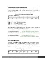
The interrupt polarity control register is presented as following table. It is used to
invert the interrupt signal or not. The detail function for these control register is
described as below.
Table 5-8: Interrupt polarity control Register
(Read/Write): wBase+0x2A
Bit 7
Bit 6
Bit 5
Bit 4
Bit 3
Bit 2
Bit 1
Bit 0
0 0 0 0
×
×
INV1
INV0
INV0=0
Æ
invert signal from INT0;
INV0=1
Æ
do not invert signal from INT0;
INV1=0
Æ
invert signal from INT1;
INV1=1
Æ
do not invert signal from INT0;
The following is the partial programs for DOS C development environment
enable or disable inverting function for interrupt signal.
outportb(wBase+0x2a,0);
/* select the inverted input from all 2 channels*/
outportb(wBase+0x2a,3);
/*select the non-inverted input from all 2 channels */
outportb(wBase+0x2a,2);
/* select the inverted input of INT0 */
/* select the non-inverted input from the others */
5.2.7 D/A Data Output
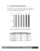
Table 5-9 and 5-10 is the output data buffer for D/A channel-1 and Table 5-11
and 5-12 is the output data buffer for D/A channel-2. These registers are write
only and user can use these to output the data through analog output CH1 and
CH2.
Table 5-9: high byte of D/A channel-1
(Write): wBase+0xc0
Bit 7
Bit 6
Bit 5
Bit 4
Bit 3
Bit 2
Bit 1
Bit 0
0 0 0 0 D11
D10
D9
D8
PISO-DA2/DA2U User Manual (Ver.2.7, Mar. 2012, PMH-020-27)
34

