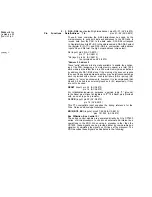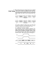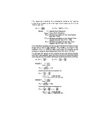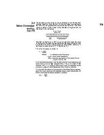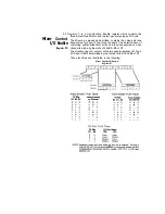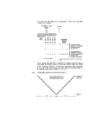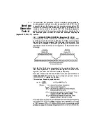
2.5 While the state flow for many microprocessors can be somewhat
State Timing
involved for certain operations, the sequence of events necessary to
control the PSG is simple and straightforward. Each of the three
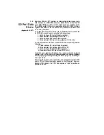
major state sequences (Latch Address, Write to PSG, and Read from
PSG) consists of several operations (indicated below by rectangular
blocks), defined by the pattern of bus control signals (BDIR, BC2,
BCl).
The functional operation and relative timing of the PSG control
sequences are described in the following paragraphs (in all exam-
ples, BC2 has been assumed to be tied to logic “1”, +5V).
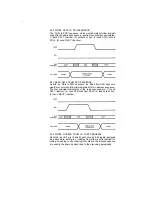
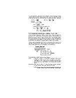
2.5.1 ADDRESS PSG REGISTER SEQUENCE
The “Latch Address.“. sequence is normally an integral part of the
write or read sequences, but for simplicity is illustrated here as an
individual sequence. Depending on the processor used the program
sequence will normally require four principal microstates: (1) send
NACT (inactive); (2) send INTAK (latch address); (3) put address on
bus: (4) send NACT (inactive). [Note: within the timing constraints
detailed in Section 7, steps (2) and (3) may be interchanged.]
Summary of Contents for ay-3-8910
Page 2: ...AY 3 8910 8912 PROGRAMMABLE SOUND GENERATOR DATA MANUAL...
Page 7: ......
Page 8: ......
Page 10: ......
Page 26: ......
Page 35: ...4 6 Interfacing to the PIC 1650 Cont...
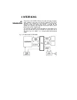
Page 36: ...Fig 19 PIC 1650 AY 3 6910 SYSTEM EXAMPLE...
Page 38: ...Fig 20 CP1600 1610 AY 3 8910 INTERFACE...
Page 40: ...Fig 21 M6800 AY 3 8910 INTERFACE...
Page 42: ......
Page 44: ......
Page 52: ...7 ELECTRICAL SPECIFICATIONS...
Page 54: ...7 ELECTRICAL SPECIFICATIONS...
Page 55: ......
Page 56: ......


