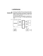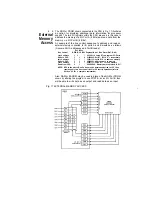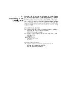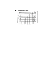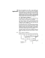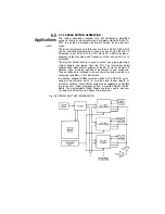
4 . 7 As shown in Fig. 20, the wiring is direct between the AY-3-8910 and a
Interfacing to the
CP1600/1610 microprocessor. The levels are compatible thus elimi-
nating any need for level converters. Even the terminology between
CP1600/1610
the IC’s remains constant to provide simple-to-follow connections.
The CP1600/1610 acts as a controller in this configuration fetching
data from ROM’s contained elsewhere in the system. The CP1600/
1610 also acts as the bus controller developing the necessary timing
for the AY-3-8910.
4.7.1 WRITE DATA ROUTINE
The program necessary to write to a selected register is as follows:
MVI value, R0; move in value to be written
MVO R0, Reg; write to register
The routine to load all registers with the same value is as follows:
MVII Reg 0, R4
CLRR R0
Here MVO@ RO, R4
CMPI Reg 0 + 17, R4
BLT Here
4.7.2 READ DATA ROUTINE
The routine to read from a selected register is as follows:
MVI Reg, RO; get data from reg in R0
MVO R0, value; store in memory
Summary of Contents for ay-3-8910
Page 2: ...AY 3 8910 8912 PROGRAMMABLE SOUND GENERATOR DATA MANUAL...
Page 7: ......
Page 8: ......
Page 10: ......
Page 26: ......
Page 35: ...4 6 Interfacing to the PIC 1650 Cont...
Page 36: ...Fig 19 PIC 1650 AY 3 6910 SYSTEM EXAMPLE...
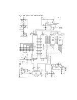
Page 38: ...Fig 20 CP1600 1610 AY 3 8910 INTERFACE...
Page 40: ...Fig 21 M6800 AY 3 8910 INTERFACE...
Page 42: ......
Page 44: ......
Page 52: ...7 ELECTRICAL SPECIFICATIONS...
Page 54: ...7 ELECTRICAL SPECIFICATIONS...
Page 55: ......
Page 56: ......

