OPERATING INSTRUCTIONS
M68HC11EVB/D
4-35
35
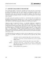
When a new source line is assembled, the assembler overwrites what was previously in memory. If
no new source line is submitted, or if there is an error in the source line, then the contents of
memory remain unchanged. Each of the instruction pairs Arithmetic Shift Left (ASL)/Logical
Shift Left (LSL) have the same opcode, so disassembly always displays the ASL mnemonic. If the
assembler tries to assemble at an address that is not in RAM, an invalid address message "rom-
xxxx" is displayed on the terminal CRT (xxxx = invalid address).
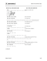
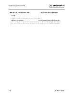
The following pages describe how to operate the assembler/disassembler by creating a typical
program loop, and debugging the program by the use of the EVB monitor commands. A typical
Serial Communications Interface (SCI) program loop is first assembled. Routine examples are
then provided to illustrate how to perform breakpoint setting, proceeding from breakpoint,
register display and modification, and initiation of user program execution.
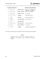
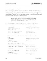
A program loop (that transmits RAM data from the SCI transmitter to the SCI receiver) is
assembled as follows:
EXAMPLE PROGRAM
PROGRAM DESCRIPTION
>BF C200 C21F 00<CR>
Clear memory space.
>ASM C000
Enter assembler/disassembler mode.
C000 CLR $0800 >LDY #C200<CR>
First byte where data is stored.
18 CE C2 00
C004 TEST >LDX #C400<CR>
Point to data to be fetched.
CE C4 00
C007 TEST >LDAA 102E<CR>
Clear RDRF bit if set.
B6 10 2E
C00A TEST >LDAA 0,X<CR>
Get first data byte.
A6 00
C00C TEST >STAA 102F<CR>
Store data in SCI data register.
B7 10 2F
C00F INX >LDAA 102E<CR>
Read SCI status register.
B6 10 2E
C012 TEST >ANDA #80<CR>
Send data byte.
84 80
C014 TEST >BEQ C00F<CR>
Wait for empty transmit data reg.
27 F9
C016 BITB $80F6 >LDAA 102E<CR>
Read SCI status register.
B6 10 2E
C019 BVS $C01B >ANDA #20<CR>
Extract RDRF bit from status reg.
84 20
(continued)
Summary of Contents for M68HC11EVB
Page 9: ...CONTENTS x M68HC11EVB D ...
Page 35: ...MONITOR PROGRAM 3 8 M68HC11EVB D ...
Page 81: ...OPERATING INSTRUCTIONS 4 46 M68HC11EVB D ...
Page 97: ...SUPPORT INFORMATION 6 12 M68HC11EVB D Figure 6 3 EVB Schematic Diagram Sheet 2 of 2 ...
Page 103: ...APPLICATIONS B 2 M68HC11EVB D Figure B 1 Single Chip Mode Configuration ...

