background image

Hardware Preparation

MVME162/D2

2-7

2

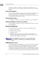
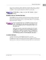
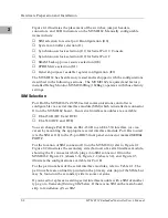
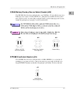
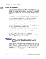
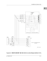
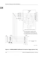
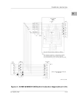
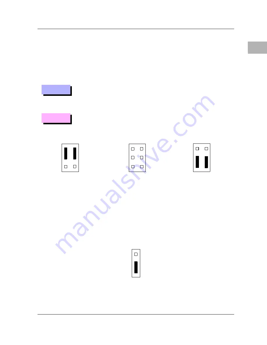
SRAM Battery Backup Source Select Header (J20)

The MVME162 is factory-configured to use 5V standby power as a 
backup power source for the SRAM (i.e., jumpers are installed across pins 1 
and 3 and 2 and 4).  To select the onboard battery as the backup power source, 
install the jumpers across pins 3 and 5 and 4 and 6.

N

ote


For MVME162s without the optional VMEbus interface (i.e.,
without the VMEchip2 ASIC), you must select the onboard
battery as the backup power source.

C

aution


Removing all jumpers may temporarily disable the SRAM.
Do not remove all jumpers from J20, except for storage.

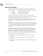
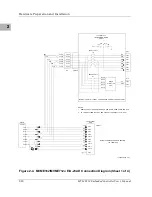
EPROM Size Select Header (J21)

The MVME162 is factory-configured for a 4Mbit EPROM (i.e., a jumper is 
installed across pins 2 and 3).  This is the only size currently available; if a 
larger EPROM becomes available, this jumper will allow it to be selected.

(Factory configuration)

5V STBY

J20

2

1

6

5

J20

2

1

6

5

J20

2

1

Backup Power Disabled

Onboard Battery

6

5

(For storage only)

1

2

3

(Factory configuration)

J21

4Mbit EPROM

Summary of Contents for MVME162

Page 1: ...MVME162 Embedded Controller User s Manual MVME162 D2 ...

Page 2: ...rior written permission of Motorola Inc It is possible that this publication may contain reference to or information about Motorola products machines and programs programming or services that are not announced in your country Such references or information must not be construed to mean that Motorola intends to announce such Motorola products programming or services in your country Restricted Right...

Page 3: ... Controller This manual is intended for anyone who wants to design OEM systems supply additional capability to an existing compatible system or work in a lab environment for experimental purposes A basic knowledge of computers and digital logic is assumed To use this manual you should be familiar with the publications listed in the Related Documentation section in Chapter 1 of this manual ...

Page 4: ...ned to provide reasonable protection against such interference when operated in a commercial environment Operation of this equipment in a residential area is likely to cause interference in which case the user at the user s own expense will be required to take whatever measures necessary to correct the interference Motorola and the Motorola symbol are registered trademarks of Motorola Inc Delta Se...

Page 5: ...rsonnel must not remove equipment covers Only Factory Authorized Service Personnel or other qualified maintenance personnel may remove equipment covers for internal subassembly or component replacement or any internal adjustment Do not replace components with power cable connected Under certain conditions dangerous voltages may exist even with the power cable removed To avoid injuries always disco...

Page 6: ......

Page 7: ...neral Description 1 6 Input Output 1 6 VMEbus Interface 1 7 No VMEbus Interface Option 1 7 MCchip 1 7 Flash Memory and EPROM 1 7 IndustryPack Modules 1 8 Optional SCSI Interface 1 8 Optional LAN Ethernet Transceiver Interface 1 8 Required Equipment 1 8 MVME162Bug Firmware 1 8 MVME712 Series Transition Modules 1 9 Available Software 1 9 Related Documentation 1 10 Support Information 1 11 Manual Ter...

Page 8: ...eader J22 2 8 Installation Instructions 2 9 IP Installation on the MVME162 2 9 MVME162 Module Installation 2 10 System Considerations 2 12 CHAPTER 3 OPERATING INSTRUCTIONS Introduction 3 1 Switches and LEDs 3 1 ABORT Switch S1 3 1 RESET Switch S2 3 1 Front Panel Indicators DS1 DS4 3 2 Memory Maps 3 3 Local Bus Memory Map 3 3 Normal Address Range 3 3 Detailed I O Memory Maps 3 7 IPIC Overall Memory...

Page 9: ...rfaces 4 8 Ethernet Interface 4 8 SCSI Interface 4 9 SCSI Termination 4 9 Local Resources 4 9 Programmable Tick Timers 4 10 Watchdog Timer 4 10 Software Programmable Hardware Interrupts 4 10 Local Bus Timeout 4 10 Timing Performance 4 10 Local Bus to DRAM Cycle Times 4 11 EPROM Flash Cycle Times 4 11 SCSI Transfers 4 11 LAN DMA Transfers 4 12 Remote Status and Control 4 12 APPENDIX A SERIAL INTERC...

Page 10: ...x ...

Page 11: ...face Module Connector Side 2 4 Figure 2 3 MVME162 MVME712M EIA 232 D Connection Diagram 2 14 Figure 2 4 MVME162 MVME712x EIA 232 D Connection Diagram 2 20 Figure 2 5 MVME162 EIA 530 Connection Diagram 2 24 Figure 4 1 MVME162 Main Module Block Diagram 4 13 Figure 4 2 Parity DRAM Mezzanine Module Block Diagram 4 14 ...

Page 12: ...xii ...

Page 13: ...3 16 Table 3 8 IPIC Overall Memory Map 3 17 Table 3 9 IPIC Memory Map Control and Status Registers 3 18 Table 3 10 MK48T08 BBRAM TOD Clock Memory Map 3 19 Table 3 11 BBRAM Configuration Area Memory Map 3 19 Table 3 12 TOD Clock Memory Map 3 20 Table 4 1 DRAM Performance 4 11 Table A 1 EIA 232 D Interconnections A 2 Table A 2 EIA 232 D Interface Transmitter Characteristics A 3 Table A 3 EIA 232 D I...

Page 14: ...xiv ...

Page 15: ...microprocessor 4MB DRAM Ethernet 512KB SRAM 013 MC68LC040 microprocessor 4MB DRAM SCSI Ethernet 512KB SRAM 014 MC68LC040 microprocessor 4MB DRAM Ethernet no VMEbus 020 MC68040 microprocessor 4MB DRAM 512KB SRAM 021 MC68040 microprocessor 4MB DRAM SCSI 512KB SRAM 022 MC68040 microprocessor 4MB DRAM Ethernet 512KB SRAM 023 MC68040 microprocessor 4MB DRAM SCSI Ethernet 512KB SRAM 026 MC68040 micropro...

Page 16: ...ers and programmable Watchdog Timer MCchip Two 32 bit programmable timers and programmable Watchdog Timer optional VMEchip2 8K by 8 Non Volatile Random Access Memory NVRAM and Time of Day TOD clock with battery backup Thompson MK48T08 Input Output Two serial ports one EIA 232 D DCE one EIA 232 D or EIA 530 DCE DTE Serial port controller Zilog Z85230 Optional Small Computer Systems Interface SCSI b...

Page 17: ...he following sections on Cooling Requirements and Special Considerations for Elevated Temperature Operation Table 1 2 MVME162 Specifications Characteristics Specifications Power requirements with PROM without IPs 5V 5 3 5 A typical 4 5 A maximum 12 Vdc 5 100 mA maximum 12 Vdc 5 100 mA maximum Operating temperature 0 to 70 C exit air with forced air cooling see NOTE Storage temperature 40 to 85 C R...

Page 18: ...t sources adequate cooling can usually be achieved with 10 CFM and 490 LFM flowing over the controller Less airflow is required to cool the controller in environments having lower maximum ambients Under more favorable thermal conditions it may be possible to operate the controller reliably at higher than 55 C with increased airflow It is important to note that there are several factors in addition...

Page 19: ...de of the board 2 Avoid placing boards with high power dissipation adjacent to the MVME162 3 Use low power IP modules only The preferred locations for IP modules are position a J2 and J3 and position d J18 and J19 FCC Compliance The MVME162 was tested without IndustryPacks in an FCC compliant chassis and meets the requirements for Class A equipment FCC compliance was achieved under the following c...

Page 20: ...P2 adapter board or LCP2 adapter board routes the signals and grounds from connector P2 to an MVME712 series transition module MVME712 12 MVME712 13 MVME712A MVME712AM or MVME712M The transition module routes the signals to the appropriate configuration headers and industry standard connectors Refer to the MVME712 12 MVME712 13 MVME712A MVME712AM and MVME712B Transition Modules and LCP2 Adapter Bo...

Page 21: ...LT or D64 MBLT No VMEbus Interface Option If desired the MVME162 can function as an embedded controller without a VMEbus interface i e without the optional VMEchip2 Contact your local Motorola sales office for ordering information MCchip The Memory Controller MCchip ASIC provides four 32 bit programmable tick timers and an interface to the LAN chip SCSI chip serial port chip BBRAM PROM Flash SRAM ...

Page 22: ...ansceiver interface for the MVME162 Required Equipment The following equipment is required to complete an MVME162 system System console terminal Disk drives and controllers Operating system MVME712 series transition module MVME712 12 MVME712 13 MVME712A MVME712AM MVME712B or MVME712M P2 Adapter Board or LCP2 Adapter Board and cable Note The MVME712B is an optional device used with MVME712 12 MVME7...

Page 23: ...equired Caution Connect peripheral devices to MVME712 serial ports 2 and 4 only Serial port 2 is the terminal or bug interface Do not connect peripheral devices to serial ports 1 and 3 or to the printer port An I O device may be connected to serial port 1 or 2 on the MVME162 or to serial port 2 or 4 on the MVME712 but not to both ports That is if an I O device is connected to MVME162 port 1 no oth...

Page 24: ...nual The MVME1x7 Data Sheet Package is composed of vendor supplied data sheets and manuals for the peripheral controllers used on the MVME162 and other boards Document Title Motorola Publication Number M68040 Microprocessors User s Manual M68040UM MVME162 Embedded Controller Support Information Refer to the Support Information section in this chapter SIMVME162 MVME162Bug Debugging Package User s M...

Page 25: ... 296853 Intel Corporation Literature Sales P O Box 58130 Santa Clara CA 95052 8130 NCR 53C710 SCSI I O Processor Data Manual order number NCR53C710DM and NCR 53C710 SCSI I O Processor Programmer s Guide order number NCR53C710PG NCR Corporation Microelectronics Products Division Colorado Springs CO MK48T08 B Timekeeper and 8Kx8 Zeropower RAM data sheet in Static RAMs Databook Order Code DBSRAM71 SG...

Page 26: ...ual assertion and negation are used to specify forcing a signal to a particular state In particular assertion and assert refer to a signal that is active or true negation and negate indicate a signal that is inactive or false These terms are used independently of the voltage level high or low that they represent In this manual MVME712 series transition module refers generically to the MVME712 12 M...

Page 27: ... are present Save the packing material for storing and reshipping of equipment Caution Avoid touching areas of integrated circuitry static discharge can damage circuits Hardware Preparation To produce the desired configuration and ensure proper operation of the MVME162 you may need to carry out certain modifications before installing the module The MVME162 provides software control over most optio...

Page 28: ...ch is installed at connector J10 on the MVME162 board Four serial interface modules are available EIA 232 D DCE and DTE EIA 530 DCE and DTE You can change Port B from an EIA 232 D to an EIA 530 interface or vice versa by mounting the appropriate serial interface module Port B is routed via the SIM at J10 to the 25 pin DB25 front panel connector marked SERIAL PORT 2 For the location of SIM connecto...

Page 29: ...0 1 2 J6 19 20 J4 DS3 DS2 DS1 1 2 1 2 J1 49 50 24 25 27 26 2 1 J3 49 F1 F2 39 2 1 P3 J8 J2 J7 40 39 2 1 P4 J14 J19 J13 J18 2 1 4 J12 2 1 4 J11 40 39 2 1 J10 J21 J20 1 2 5 6 1 15 16 J22 SERIAL PORT 2 SERIAL PORT 1 CONSOLE STAT FAIL RUN SCON LAN FUSE SCSI VME ABORT RESET 49 50 1 2 J16 49 50 1 2 J17 49 50 24 25 27 26 2 1 49 50 24 25 27 26 2 1 49 50 24 25 27 26 2 1 49 50 24 25 27 26 2 1 49 50 24 25 27...

Page 30: ...n a safe place for later use 2 Grasp opposite sides of the SIM and gently lift straight up Caution Avoid lifting the SIM by one side only as the connector can be damaged on the SIM or the main board 3 Place the SIM in a static safe container for possible reuse Table 2 1 Serial Interface Module Part Numbers EIA Standard Configuration Part Number Model Number EIA 232 D DTE 01 W3846B SIM05 DCE 01 W38...

Page 31: ...screws that you previously removed or that were supplied with the new SIM into the two opposite corner mounting holes Screw them into the standoffs but do not overtighten them The signal relationships and signal connections in the various serial configurations available for ports A and B are illustrated in Figures 2 3 2 4 and 2 5 System Controller Select Header J1 The MVME162 is factory configured...

Page 32: ...SERIAL PORT 1 CONSOLE connection install jumpers across pins 1 and 2 and pins 3 and 4 Clock Select Header J12 for Serial Port 2 The MVME162 is shipped from the factory with the SERIAL PORT 2 header configured for asynchronous communications i e jumpers removed To select synchronous communications for the SERIAL PORT 2 connection install jumpers across pins 1 and 2 and pins 3 and 4 J11 J11 External...

Page 33: ...out the VMEchip2 ASIC you must select the onboard battery as the backup power source Caution Removing all jumpers may temporarily disable the SRAM Do not remove all jumpers from J20 except for storage EPROM Size Select Header J21 The MVME162 is factory configured for a 4Mbit EPROM i e a jumper is installed across pins 2 and 3 This is the only size currently available if a larger EPROM becomes avai...

Page 34: ...jumpers are user definable pins 1 2 3 4 5 6 7 8 11 12 13 14 15 16 Note Pins 9 10 GPIO3 are reserved to select either the Flash memory map jumper installed or the EPROM memory map jumper removed They are not user definable The MVME162 is shipped from the factory with J22 set to all zeros jumpers on all pins J22 15 GPIO7 GPIO6 GPIO5 GPIO1 GPIO4 GPIO3 GPIO2 1 2 16 GPIO0 EPROMs Selected factory config...

Page 35: ...into connectors J2 and J3 plug IP_b into J7 and J8 Plug IP_c into J13 and J14 plug IP_d into J18 and J19 If a double sized IP is used plug IP_ab into J2 J3 J7 and J8 plug IP_cd into J13 J14 J18 and J19 2 Four additional 50 pin connectors J6 J5 J17 and J16 are provided behind the MVME162 front panel for external cabling connections to the IP modules There is a one to one correspondence between the ...

Page 36: ...s system controller it must occupy the leftmost card slot slot 1 The system controller must be in slot 1 to correctly initiate the bus grant daisy chain and to ensure proper operation of the IACK daisy chain driver If you do not intend to use the MVME162 as system controller it can occupy any unused double height card slot 4 Slide the MVME162 into the selected card slot Be sure the module is seate...

Page 37: ...tion module They are in compatible with the EIA 530 interface refer to MVME162 Serial Port 2 in Chapter 4 Functional Description 9 Connect the appropriate cable s to the panel connectors for the EIA 232 D serial ports SCSI port and LAN Ethernet port Note that some cables are not provided with the MVME712 series module and must be made or purchased by the user Motorola recommends shielded cable for...

Page 38: ...ress Refer to theMVME162 Embedded Controller Programmer s Reference Guide for more information If the MVME162 tries to access offboard resources in a nonexistent location and is not system controller and if the system does not have a global bus timeout the MVME162 waits forever for the VMEbus cycle to complete This will cause the system to lock up There is only one situation in which the system mi...

Page 39: ...e When the MVME712M module is used the yellow DS1 LED on the MVME712M illuminates when LAN power is available which indicates that the fuse is good If the Ethernet transceiver fails to operate check fuse F2 The MVME162 provides SCSI terminator power through a 1A fuse F1 located on the P2 Adapter Board or LCP2 Adapter Board If the fuse is blown the SCSI device s may function erratically or not at a...

Page 40: ... TXD RXD RTS CTS DTR DCD TXC RXC TXD RXD RTS CTS DTR DCD 1 5K TXD RXD RTS CTS DTR DCD DSR TXC 1 3 2 4 J11 RXC TXCO PIN 2 PIN 3 PIN 4 PIN 5 PIN 20 PIN 8 PIN 6 PIN 15 PIN 17 PIN 24 PIN 7 DB25 PIN 2 PIN 3 PIN 4 PIN 5 PIN 20 PIN 8 PIN 6 PIN 15 PIN 17 PIN 24 PIN 7 TO MODEM J17 TO TERMINAL J16 P2 CABLE RXD TXD CTS RTS DCD DTR MVME 712M EIA 232 D DTE CONFIGURATION TO MODEM 712M TRANSITION MODULE PORT 2 M...

Page 41: ...CD TXC RXC TXD RXD RTS CTS DTR DCD 1 5K TXD RXD RTS CTS DTR DCD DSR TXC 1 3 2 4 J11 RXC TXCO PIN 2 PIN 3 PIN 4 PIN 5 PIN 20 PIN 8 PIN 6 PIN 15 PIN 17 PIN 24 PIN 7 DB25 PIN 2 PIN 3 PIN 4 PIN 5 PIN 20 PIN 8 PIN 6 PIN 15 PIN 17 PIN 24 PIN 7 TO MODEM J17 TO TERMINAL J16 P2 CABLE RXD TXD CTS RTS DCD DTR MVME712M EIA 232 D DCE CONFIGURATION TO TERMINAL 712M TRANSITION MODULE PORT 2 MVME162 EIA 232 D DCE...

Page 42: ...3 J12 RXC TXCO PIN 2 PIN 3 PIN 4 PIN 5 PIN 20 PIN 8 PIN 6 PIN 15 PIN 17 PIN 24 PIN 7 DB25 PIN 2 PIN 3 PIN 4 PIN 5 PIN 20 PIN 8 PIN 6 PIN 15 PIN 17 PIN 24 PIN 7 TO MODEM J19 TO TERMINAL J18 P2 CABLE TXD RXD RTS CTS DTR DCD MVME712M EIA 232 D DTE CONFIGURATION TO MODEM 712M TRANSITION MODULE PORT 4 MVME 162 EIA 232 D DTE CONFIGURATION TO MODEM 10970 00 3 6 9405 DSR TXC RXC TXCO DB25 SIM05 5V 1 4 2 J...

Page 43: ...CD 1 5K TXD RXD RTS CTS DTR DCD DSR TXC 3 J12 RXC TXCO PIN 2 PIN 3 PIN 4 PIN 5 PIN 20 PIN 8 PIN 6 PIN 15 PIN 17 PIN 24 PIN 7 DB25 PIN 2 PIN 3 PIN 4 PIN 5 PIN 20 PIN 8 PIN 6 PIN 15 PIN 17 PIN 24 PIN 7 TO MODEM J19 TO TERMINAL J18 P2 CABLE TXD RXD RTS CTS DTR DCD MVME 162 EIA 232 D DCE CONFIGURATION TO TERMINAL 10970 00 4 6 9405 DSR TXC RXC TXCO DB25 5V 1 4 2 J15 P2 A32 P2 A28 RTXC TRXC RTXC4 TRXC4 ...

Page 44: ...IN 7 DB25 PIN 2 PIN 3 PIN 4 PIN 5 PIN 20 PIN 8 PIN 6 PIN 15 PIN 17 PIN 24 PIN 7 TO MODEM J19 TO TERMINAL J18 P2 CABLE TXD RXD RTS CTS DTR DCD MVME712M EIA 232 D CONFIGURATION TO TERMINAL MVME 162 EIA 232 D DTE CONFIGURATION TO MODEM 10970 00 5 6 9405 DSR TXC RXC TXCO DB25 5V 1 4 2 J15 P2 A32 P2 A28 RTXC TRXC 1 WITH DTE MODULE AND MVME 712 JUMPERED AS TO TERMINAL THE CLOCKS TXC AND RXC ARE THE WRON...

Page 45: ... 3 PIN 4 PIN 5 PIN 20 PIN 8 PIN 6 PIN 15 PIN 17 PIN 24 PIN 7 TO MODEM J19 TO TERMINAL J18 P2 CABLE TXD RXD RTS CTS DTR DCD MVME712M EIA 232 D DTE CONFIGURATION TO MODEM MVME 162 EIA 232 D DCE CONFIGURATION TO TERMINAL 10970 00 6 6 9405 DSR TXC RXC TXCO DB25 J15 P2 A32 P2 A28 RTXC TRXC WITH DCE MODULE AND MVME 712 JUMPERED AS TO TERMINAL THE CLOCKS TXC AND RXC ARE THE WRONG DIRECTION RTXC4 TRXC4 TH...

Page 46: ... J11 RXC TXCO PIN 2 PIN 3 PIN 4 PIN 5 PIN 20 PIN 8 PIN 6 PIN 15 PIN 17 PIN 24 PIN 7 DB25 SERIAL PORT 2 MODEM PORT 2 J17 P2 RXD TXD CTS RTS DCD DTR MVME 712A AM 12 13 PORT 2 CONFIGURED AS EIA 232 D SERIAL PORT 712A AM 12 13 TRANSITION MODULE PORT 2 MVME162 RS232 DCE CONFIGURATION TO TERMINAL 11020 00 9406 1 4 DSR CABLE MTXD J16 PIN 3 PIN 2 PIN 7 PIN 8 PIN 4 PIN 1 PIN 6 PIN 2 PIN 3 DB9 1 5K J9 DCE D...

Page 47: ...NG RJ11 FRONT PANEL P2 C27 P2 C28 P2 C29 P2 C30 P2 C31 P2 C32 TXD2 RXD2 RTS2 CTS2 DTR2 DCD2 PORT 1 D R D D D D D R R R Z85230 A PORT TXD RXD RTS CTS DTR DCD TXC RXC TXD RXD RTS CTS DTR DCD DSR TXC 1 3 2 4 J11 RXC TXCO PIN 2 PIN 3 PIN 4 PIN 5 PIN 20 PIN 8 PIN 6 PIN 15 PIN 17 PIN 24 PIN 7 DB25 P2 CABLE RXD TXD CTS RTS DCD DTR MVME162 RS232 DCE CONFIGURATION TO TERMINAL 11020 00 9406 2 4 5 12 12Vdc B...

Page 48: ...E 2 TO CONNECT TERMINAL SET DSR LINE PULLUP SELECT J14 TO DCE FRONT PANEL P2 A25 P2 A26 P2 A27 P2 A29 P2 A30 P2 A31 TXD4 RXD4 RTS4 CTS4 DTR4 DCD4 PORT 2 D R D D D R R R Z85230 B PORT TXD RXD RTS CTS DTR DCD TXC RXC TXD RXD RTS CTS DTR DCD DSR TXC 3 J12 RXC TXCO PIN 2 PIN 3 PIN 4 PIN 5 PIN 20 PIN 8 PIN 6 PIN 15 PIN 17 PIN 24 PIN 7 DB25 P2 CABLE TXD RXD RTS CTS DTR DCD MVME 162 RS232 DTE CONFIGURATI...

Page 49: ... SET DSR LINE PULLUP SELECT J14 TO DCE NC NC PIN 3 PIN 2 PIN 7 PIN 8 PIN 4 PIN 1 PIN 6 DB9 FRONT PANEL P2 A25 P2 A26 P2 A27 P2 A29 P2 A30 P2 A31 TXD4 RXD4 RTS4 CTS4 DTR4 DCD4 PORT 2 D R D D D D D R R R Z85230 B PORT TXD RXD RTS CTS DTR DCD TXC RXC TXD RXD RTS CTS DTR DCD DSR TXC 3 J12 RXC TXCO PIN 2 PIN 3 PIN 4 PIN 5 PIN 20 PIN 8 PIN 6 PIN 15 PIN 17 PIN 24 PIN 7 DB25 P2 CABLE TXD RXD RTS CTS DTR D...

Page 50: ..._B RXC_A TXCO_B TXCO_A TM_A LL_A RL_A PIN 1 PIN 14 PIN 2 PIN 16 PIN 3 PIN 18 PIN 4 PIN 13 PIN 5 PIN 23 PIN 20 PIN 10 PIN 8 PIN 22 PIN 6 PIN 12 PIN 15 PIN 9 PIN 17 PIN 11 PIN 24 PIN 25 PIN 19 PIN 21 PIN 7 PORT FRONT PANEL DB 25 R D NC D 5V 5V NC R R R D R R RTS 2 1 3 J12 D 5V NC 2 P2 CONNECTOR P2 C18 P2 A25 P2 A19 P2 A26 P2 C19 P2 A27 P2 C26 P2 A29 P2 A23 P2 A30 P2 C22 P2 A31 P2 A22 P2 A20 P2 C24 P...

Page 51: ...PORT FRONT PANEL DB 25 Z85230 B PORT TXD RXD CTS DTR DCD TXC RXC 2 1 3 J12 5V NC 2 P2 CONNECTOR P2 C18 P2 A25 P2 A19 P2 A26 P2 C19 P2 A27 P2 C26 P2 A29 P2 A23 P2 A30 P2 C22 P2 A31 P2 A22 P2 A20 P2 C24 P2 A32 P2 C21 P2 A28 P2 C23 P2 A24 P2 C25 P2 C20 P2 A21 D R D R D R D D D R D 5V NC NC PIN 7 PIN 1 PIN 14 PIN 2 PIN 16 PIN 3 PIN 13 PIN 5 PIN 23 PIN 20 PIN 10 PIN 8 PIN 22 PIN 6 PIN 12 PIN 15 PIN 9 P...

Page 52: ...Hardware Preparation and Installation 2 26 MVME162 Embedded Controller User s Manual 2 ...

Page 53: ...This interrupter is filtered to remove switch bounce RESET Switch S2 The RESET switch resets all onboard devices it also drives SYSRESET if the MVME162 is the system controller The RESET switch may be disabled by software The VMEchip2 includes both a global and a local reset driver When the VMEchip2 operates as the VMEbus system controller the reset driver provides a global system reset by asserti...

Page 54: ...on the MVME162 Lights when a halt condition from the processor is detected Part of DS1 RUN LED green Lights when the local bus TIP signal line is low This indicates one of the local bus masters is executing a local bus cycle Part of DS2 SCON LED green Lights when the VMEchip2 in the MVME162 is the VMEbus system controller Part of DS2 LAN LED green Lights when the LAN chip is local bus master Part ...

Page 55: ...cknowledge codes Normal Address Range The memory map of devices that respond to the normal address range is shown in the following tables The normal address range is defined by the TT signals on the local bus For the MVME162 transfer types 0 1 and 2 define the normal address range Table 3 1 defines the entire map 00000000 to FFFFFFFF Many areas of the map are user programmable and suggested uses a...

Page 56: ...ximate 4 Cache inhibit depends on devices in area mapped Table 3 1 Local Bus Memory Map Address Range Devices Accessed Port Width Size Software Cache Inhibit Notes Programmable DRAM on Board D32 1MB 8MB N 2 Programmable SRAM D32 128KB 2MB N 2 Programmable VMEbus A32 A24 D32 D16 4 Programmable IP_a Memory D32 D8 64 KB 8 MB 2 4 Programmable IP_b Memory D32 D8 64 KB 8 MB 2 4 Programmable IP_c Memory ...

Page 57: ...f they are not decoded an access to this address range will generate a local bus timeout The local bus timer must be enabled Table 3 2 focuses on the Local I O Devices portion of the local bus main memory map Table 3 2 Local I O Devices Memory Map Address Range Devices Accessed Port Width Size Notes FFF00000 FFF3FFFF Reserved 256 KB 4 FFF40000 FFF400FF VMEchip2 LCSR D32 256 B 1 3 FFF40100 FFF401FF...

Page 58: ...16 256 B 8 FFF58800 FFF5887F Reserved 128 B 1 FFF58880 FFF588FF Reserved 128 B 1 FFF58900 FFF5897F Reserved 128 B 1 FFF58980 FFF589FF Reserved 128 B 1 FFF58A00 FFF58A7F Reserved 128 B 1 FFF58A80 FFF58AFF Reserved 128 B 1 FFF58B00 FFF58B7F Reserved 128 B 1 FFF58B80 FFF58BFF Reserved 128 B 1 FFF58C00 FFF58CFF Reserved 256 B 1 FFF58D00 FFF58DFF Reserved 256 B 1 FFF58E00 FFF58EFF Reserved 256 B 1 FFF5...

Page 59: ...timer is enabled the access times out and is terminated by a TEA signal 5 Size is approximate 6 Port commands to the 82596CA must be written as two 16 bit writes upper word first and lower word second 7 Refer to the Flash and EPROM Interface section in the MCchip description in Chapter 3 Detailed I O Memory Maps Tables 3 3 through 3 12 provide detailed memory maps for the VMEchip2 the MCchip the Z...

Page 60: ...STER ADDRESS TRANSLATION ADDRESS 4 VMEchip2 LCSR Base Address FFF40000 OFFSET 16 17 18 19 20 21 22 23 24 25 26 27 28 29 30 31 16 17 18 19 20 21 22 23 24 25 26 27 28 29 30 31 16 17 18 19 20 21 22 23 24 25 26 27 28 29 30 31 MAST D16 EN MAST WP EN MAST D16 EN MAST WP EN MASTER AM 3 MASTER AM 4 GCSR GROUP SELECT GCSR BOARD SELECT MAST 4 EN MAST 3 EN MAST 2 EN MAST 1 EN TICK 2 1 TICK IRQ 1 EN CLR IRQ I...

Page 61: ...SLATION SELECT 2 0 1 2 3 4 5 6 7 8 9 10 11 12 13 14 15 0 1 2 3 4 5 6 7 8 9 10 11 12 13 14 15 IO2 EN IO2 WP EN IO2 S U IO2 P D IO1 EN IO1 D16 EN IO1 WP EN IO1 S U 0 1 2 3 4 5 6 7 8 9 10 11 12 13 14 15 MASTER AM 2 MASTER AM 1 ROM SIZE ROM BANK B SPEED ROM BANK A SPEED DMA TBL INT DMA LB SNP MODE DMA INC VME DMA INC LB DMA D64 BLK DMA BLK DMA AM 5 DMA AM 4 DMA WRT DMA D16 DMA AM 3 DMA AM 2 DMA AM 1 D...

Page 62: ...IRQ TIC2 IRQ TIC1 IRQ VME IACK IRQ DMA IRQ SIG3 IRQ SIG2 IRQ SIG1 IRQ SIG0 IRQ LM1 IRQ LM0 IRQ ABORT IRQ LEVEL SYS FAIL IRQ LEVEL MST WP ERROR IRQ LEVEL VME IACK IRQ LEVEL DMA IRQ LEVEL SIG 3 IRQ LEVEL SIG 2 IRQ LEVEL SW7 IRQ LEVEL SW6 IRQ LEVEL SW5 IRQ LEVEL SW4 IRQ LEVEL SPARE IRQ LEVEL VME IRQ 7 IRQ LEVEL VME IRQ 6 IRQ LEVEL VME IRQ 5 IRQ LEVEL VECTOR BASE REGISTER 0 VECTOR BASE REGISTER 1 MST ...

Page 63: ...2 CLR IRQ 11 CLR IRQ 10 CLR IRQ 9 CLR IRQ 8 SET IRQ 15 SET IRQ 14 SET IRQ 13 SET IRQ 12 SET IRQ 11 SET IRQ 10 SET IRQ 9 SET IRQ 8 SW7 IRQ SW6 IRQ SW5 IRQ SW4 IRQ SW3 IRQ SW2 IRQ SW1 IRQ SW0 IRQ SPARE VME IRQ7 VME IRQ6 VME IRQ5 VME IRQ4 VME IRQ3 VME IRQ2 VME IRQ1 0 1 2 3 4 5 6 7 8 9 10 11 12 13 14 15 GPIOO P ERROR IRQ LEVEL IRQ1E IRQ LEVEL TIC TIMER 2 IRQ LEVEL TIC TIMER 1 IRQ LEVEL SW3 IRQ LEVEL S...

Page 64: ...Operating Instructions 3 12 User s Manual 3 This page intentionally left blank ...

Page 65: ...VISION CHIP ID 2 4 LM3 LM2 LM1 LM0 SIG3 SIG2 SIG1 SIG0 RST ISF BF SCON SYSFL X X X 4 8 GENERAL PURPOSE CONTROL AND STATUS REGISTER 0 6 C GENERAL PURPOSE CONTROL AND STATUS REGISTER 1 8 10 GENERAL PURPOSE CONTROL AND STATUS REGISTER 2 A 14 GENERAL PURPOSE CONTROL AND STATUS REGISTER 3 C 18 GENERAL PURPOSE CONTROL AND STATUS REGISTER 4 E 1C GENERAL PURPOSE CONTROL AND STATUS REGISTER 5 ...

Page 66: ...y Error Interrupt Control SCC Interrupt Control Tick Timer 4 Control Tick Timer 3 Control 20 DRAM Space Base Address Register SRAM Space Base Address Register 24 DRAM Space Size DRAM SRAM Options SRAM Space Size Reserved 28 LANC Error Status Reserved LANC Interrupt Control LANC Bus Error Interrupt Control 2C SCSI Error Status General Purpose Inputs MVME162 Version SCSI Interrupt Control 30 Tick Ti...

Page 67: ...er Writes to the System Configura tion Pointer must be upper word first lower word second Table 3 5 Z85230 SCC Register Addresses SCC SCC Register Address SCC 1 Port B Control FFF45001 Port B Data FFF45003 Port A Control FFF45005 Port A Data FFF45007 SCC 2 Port B Control FFF45801 Port B Data FFF45803 Port A Control FFF45805 Port A Data FFF45807 Table 3 6 82596CA Ethernet LAN Memory Map Data Bits A...

Page 68: ... Big Endian Mode SCRIPTs and Little Endian Mode 00 SIEN SDID SCNTL1 SCNTL0 00 04 SOCL SODL SXFER SCID 04 08 SBCL SBDL SIDL SFBR 08 0C SSTAT2 SSTAT1 SSTAT0 DSTAT 0C 10 DSA 10 14 CTEST3 CTEST2 CTEST1 CTEST0 14 18 CTEST7 CTEST6 CTEST5 CTEST4 18 1C TEMP 1C 20 LCRC CTEST8 ISTAT DFIFO 20 24 DCMD DBC 24 28 DNAD 28 2C DSP 2C 30 DSPS 30 34 SCRATCH 34 38 DCNTL DWT DIEN DMODE 38 3C ADDER 3C ...

Page 69: ...FF580C0 FFF580FF IP_a ID Space Repeated D16 64 B FFF58100 FFF5817F IP_b I O Space D16 128 B FFF58180 FFF581BF IP_b ID Space D16 64 B FFF581C0 FFF581FF IP_b ID Space Repeated D16 64 B FFF58200 FFF5827F IP_c I O Space D16 128 B FFF58280 FFF582BF IP_c ID Space D16 64 B FFF582C0 FFF582FF IP_c ID Space Repeated D16 64 B FFF58300 FFF5837F IP_d I O Space D16 128 B FFF58380 FFF583BF IP_d ID Space D16 64 B...

Page 70: ...ER d_BASE31 d_BASE30 d_BASE29 d_BASE28 d_BASE27 d_BASE26 d_BASE25 d_BASE24 0B IP_d MEM BASE LOWER d_BASE23 d_BASE22 d_BASE21 d_BASE20 d_BASE19 d_BASE18 d_BASE17 d_BASE16 0C IP_a MEM SIZE a_SIZE23 a_SIZE22 a_SIZE21 a_SIZE20 a_SIZE19 a_SIZE18 a_SIZE17 a_SIZE16 0D IP_b MEM SIZE b_SIZE23 b_SIZE22 b_SIZE21 b_SIZE20 b_SIZE19 b_SIZE18 b_SIZE17 b_SIZE16 0E IP_c MEM SIZE c_SIZE23 c_SIZE22 c_SIZE21 c_SIZE20...

Page 71: ...ting System Area 1528 FFFC16F8 FFFC1EF7 Debugger Area 2048 FFFC1EF8 FFFC1FF7 Configuration Area 256 FFFC1FF8 FFFC1FFF TOD Clock 8 Table 3 11 BBRAM Configuration Area Memory Map Address Range Description Size Bytes FFFC1EF8 FFFC1EFB Version 4 FFFC1EFC FFFC1F07 Serial Number 12 FFFC1F08 FFFC1F17 Board ID 16 FFFC1F18 FFFC1F27 PWA 16 FFFC1F28 FFFC1F2B Speed 4 FFFC1F2C FFFC1F31 Ethernet Address 6 FFFC1...

Page 72: ... 8 FFFC1F7E FFFC1F85 IP_b Board PWB 8 FFFC1F86 FFFC1F8D IP_c Board ID 8 FFFC1F8E FFFC1F95 IP_c Board Serial Number 8 FFFC1F96 FFFC1F9D IP_c Board PWB 8 FFFC1F9E FFFC1FA5 IP_d Board ID 8 FFFC1FA6 FFFC1FAD IP_d Board Serial Number 8 FFFC1FAE FFFC1FB5 IP_d Board PWB 8 FFFC1FB6 FFFC1FF6 Reserved 65 FFFC1FF7 Checksum 1 Table 3 12 TOD Clock Memory Map Data Bits Address D7 D6 D5 D4 D3 D2 D1 D0 Function F...

Page 73: ...debugger MVME162Bug The fifth area detailed in Table 3 11 is the configuration area The sixth area the TOD clock detailed in Table 3 12 is defined by the chip hardware The data structure of the configuration bytes starts at FFFC1EF8 and is as follows struct brdi_cnfg char version 4 char serial 12 char id 16 char pwa 16 char speed 4 char ethernet 6 char fill 2 char lscsiid 2 char mem_pwb 8 char mem...

Page 74: ... for a set Additional boards in a set are defined by a structure for that set For example for an MVME162 board with MC68040 SCSI Ethernet 4MB DRAM and 512KB SRAM at revision A the PWA field contains 01 W3814B01A The 12 characters are followed by four blanks 5 Four bytes contain the speed of the board in MHz The first two bytes are the whole number of MHz and the second two bytes are fractions of M...

Page 75: ...e printed wiring board PWB number assigned to the optional second IndustryPack b 19 Eight bytes are reserved for the board identifier in ASCII format assigned to the optional third IndustryPack c 20 Eight bytes are reserved for the serial number in ASCII format assigned to the optional third IndustryPack c 21 Eight bytes are reserved for the printed wiring board PWB number assigned to the optional...

Page 76: ...grammable map decoder for the GCSR The GCSR map decoder allows you to program the starting address of the GCSR in the VMEbus short I O space Software Initialization Most functions that have been done with switches or jumpers on other modules are done by setting control registers on the MVME162 At powerup or reset the EPROMs that contain the 162Bug debugging package set up the default values of man...

Page 77: ...is a partial system reset not a complete system reset such as powerup reset or SYSRESET When the local bus reset signal is asserted a local bus cycle may be aborted The VMEchip2 is connected to both the local bus and the VMEbus and if the aborted cycle is bound for the VMEbus erratic operation may result Communications between the local processor and a VMEbus master should use interrupts or mailbo...

Page 78: ...Operating Instructions 3 26 User s Manual 3 ...

Page 79: ...MB 4MB or 8MB of DRAM 512KB of SRAM 1MB Flash memory four MVIP IndustryPack interfaces and two serial ports one EIA 232 D DCE one EIA 232 D or EIA 530 DCE DTE Options include an SCSI mass storage interface a LAN Ethernet transceiver interface and a non VMEbus version Data Bus Structure The local data bus on the MVME162 is a 32 bit synchronous bus that is based on the MC68040 bus and which supports...

Page 80: ... can be found in the section on the SRAM Memory Controller in the MCchip Programming Model in the MVME162 Embedded Controller Programmer s Reference Guide The SRAM arrays are not parity protected The battery backup function for the MVME162 SRAM is provided by a Dallas DS1210S device that supports primary and secondary power sources In the event of a main board power failure the DS1210S checks powe...

Page 81: ...hium battery supplied on the MVME162 should provide at least two years of backup time with the board powered off and with an ambient temperature of 40 C If the power on duty cycle is 50 the board is powered on half of the time the battery lifetime is four years At lower ambient temperatures the backup time is significantly longer and may approach the shelf life of the battery When a board is store...

Page 82: ...ering is required Onboard DRAM The MVME162 offers a 1MB a 4MB and an 8MB DRAM option The DRAM architecture is non interleaved for 1MB and interleaved for 4MB and 8MB Parity protection can be enabled with interrupts or bus exception when a parity error is detected DRAM performance is specified in the section on the DRAM Memory Controller in the MCchip Programming Model in the MVME162 Embedded Contr...

Page 83: ...mmer s Reference Guide for detailed programming information Refer to the MVME162 Embedded Controller Support Information manual for the pin assignments of VMEbus backplane connectors P1 and P2 Note that the ABORT switch logic in the VMEchip2 is not used The GPI inputs to the VMEchip2 which are located at FFF40088 bits 7 0 are not used The ABORT switch interrupt is integrated into the MCchip ASIC a...

Page 84: ...connected to the TxC and RxC clock signals which may be present on the DB25 connector These connections are made via header J11 on the MVME162 board see Figures 2 3 and 2 4 in Chapter 2 The TxC and RxC clocks are not available at Port 2 on the MVME712 series transition modules On MVME712x transition modules Port 2 can be routed either through a DB9 DTE serial interface or if the module is so equip...

Page 85: ... be configured as either a DTE or DCE EIA 232 D serial port via jumper headers J19 and J18 on the MVME712M Port 4 can also be connected to the TxC and RxC clock signals which may be present on the DB25 connector These connections are made via header J15 on the MVME712M see Figure 2 3 sheets 3 6 in Chapter 2 When Port B is configured as an EIA 530 interface EIA 530 data transfers normally occur thr...

Page 86: ...f the IP connectors Ethernet Interface The Intel 82596CA LAN controller is used to implement the Ethernet transceiver interface The 82596CA accesses local RAM using DMA operations to perform its normal functions Because the 82596CA has small internal buffers and the VMEbus has an undefined latency period buffer overrun may occur if the DMA is programmed to access the VMEbus Therefore the 82596CA s...

Page 87: ...he SCSI interface is implemented using the NCR 53C710 SCSI I O controller Support functions for the NCR 53C710 are provided by the MCchip Refer to the NCR 53C710 user s guide and to the MVME162 Embedded Controller Programmer s Reference Guide for detailed programming information Refer to the MVME712 12 MVME712 13 MVME712A MVME712AM and MVME712B Transition Modules and LCP2 Adapter Board User s Manu...

Page 88: ...on Software Programmable Hardware Interrupts Eight software programmable hardware interrupts are provided by the VMEchip2 These interrupts allow software to create a hardware interrupt Refer to the VMEchip2 desciption in the MVME162 Embedded Controller Programmer s Reference Guide for detailed programming information Local Bus Timeout The MVME162 provides timeout functions in the VMEchip2 and the ...

Page 89: ...vary depending on the device speed The data transfers are 32 bits wide Refer to the MVME162 Embedded Controller Programmer s Reference Guide SCSI Transfers The MVME162 includes an SCSI mass storage bus interface with DMA controller The SCSI DMA controller uses a FIFO buffer to interface the 8 bit SCSI bus to the 32 bit local bus The FIFO buffer allows the SCSI DMA controller to efficiently transfe...

Page 90: ...o efficiently transfer data to the local bus The 82596CA does not execute MC68040 compatible burst cycles therefore the LAN DMA controller does not use burst transfers Parity DRAM write cycles require 3 clock cycles and read cycles require 5 clock cycles with parity off and 6 clock cycles with parity on The transfer rate of the LAN DMA controller is 20MB sec at 25 MHz with parity off Assuming a co...

Page 91: ...HES J4 IPCHIP MC68040 MPU IP MODULES BBRAM AND TOD SERIAL PORTS DRAM MEZZANINE IPL COMBINER CLOCKS GENERATOR MC CHIP EPROM SCSI INTERFACE LANCE SIA VME BUFFERS BATTERY BACKUP FLASH P1 J5 J6 J16 J17 J2 J7 J13 J18 J3 J8 J14 J19 SERIAL PORTS REMOTE RESET ABORT LEDS P3 P4 VME VME LAN SERIAL PORTS SCSI P2 J9 J15 ...

Page 92: ...Functional Description 4 14 User s Manual 4 Figure 4 1 MVME162 Main Module Block Diagram ...

Page 93: ...MVME162 Functional Description MVME162 D2 4 15 4 J1 WE LL WE LM CAS RAS OE ADDRESS PARITY WE UM WE UU J1 DATA 00 15 DATA 16 31 10685 00 9309 RAM 00 15 RAM 16 31 ...

Page 94: ...Functional Description 4 16 User s Manual 4 Figure 4 2 Parity DRAM Mezzanine Module Block Diagram ...

Page 95: ...o 38 4KB sec EIA 232 D Connections The EIA 232 D standard defines the electrical and mechanical aspects of this serial interface The interface employs unbalanced single ended signaling and is generally used with DB25 connectors although other connector styles e g DB9 and RJ45 are sometimes used as well Table A 1 lists the standard EIA 232 D interconnections Not all pins listed in the table are nec...

Page 96: ...ceive data 7 SG Signal Ground Common return line for all signals at the modem interface 8 DCD Data Carrier Detect Output from modem to terminal to indicate that a valid carrier is being received 9 14 Not used 15 TxC Transmit Clock DCE Output from modem to terminal clocks data from the terminal to the modem 16 Not used 17 RxC Receive Clock Output from terminal to modem clocks input data from the te...

Page 97: ...meters for serial binary data interchange between DTE and DCE devices using unbalanced lines EIA 232 D transmitter and receiver parameters applicable to the MVME162 are listed in Tables A 2 and A 3 Table A 2 EIA 232 D Interface Transmitter Characteristics Parameter Value Minimum Maximum Unit Output voltage with load resistance of 3000Ω to 7000Ω 8 5 V Open circuit output voltage 12 V Short circuit ...

Page 98: ...well as unbalanced single ended signaling and offers the possibility of higher data rates than EIA 232 D with the same DB25 connector Table A 4 lists the EIA 530 interconnections that are available at serial port B SERIAL PORT 2 on the front panel when the port is configured via serial interface modules as an EIA 530 DCE or DTE port Table A 3 EIA 232 D Interface Receiver Characteristics Parameter ...

Page 99: ...data 13 CTS_B Clear to Send B Input to DTE from DCE to indicate that message transmission can begin 14 TxD_B Transmit Data B Data to be transmitted output from DTE to DCE 15 TxC_A Transmit Signal Element Timing DCE A Control signal that clocks input data 16 RxD_B Receive Data B Data which is demodulated from the receive line input from DCE to DTE 17 RxC_A Receive Signal Element Timing DCE A Contro...

Page 100: ...al conductor and circuit ground at the load end of the cable with a 50Ω resistor substituted for the transmitter It is necessary to minimize interference with other signals Inversion of signals may be required e g plus polarity MARK to minus polarity MARK may be achieved by inverting the cable pair EIA 530 interface transmitter and receiver parameters applicable to the MVME162 are listed in Tables...

Page 101: ...output current for any voltage between 7V and 7V 180 mA Power off output current for any voltage between 7V and 7V 100 µA Output transition time with 100Ω 15pF load 15 ns Table A 6 EIA 530 Interface Receiver Characteristics Parameter Value Minimum Maximum Unit Differential input voltage 12 V Input offset voltage 12 V Differential input high threshold voltage 200 mV Differential input low threshold...

Page 102: ...ed to different electrical outlets there may be several volts of difference in ground potential If pin 1 of each device is interconnected with the others via cable several amperes of current could result This condition may not only be dangerous for the small wires in a typical cable but may also produce electrical noise that causes errors in data transmission That is why Tables A 1 and A 4 show no...

Page 103: ...21 control status register 2 12 cooling requirements 1 4 D data circuit terminating equipment DCE A 1 4 6 data terminal equipment DTE A 1 4 6 debugging firmware 1 8 decimal number 1 12 DRAM base address 2 12 options 4 4 E EIA 232 D interconnections A 1 SIM part numbers 2 4 EIA 530 interconnections A 4 interface characteristics 4 7 A 6 signals A 4 SIM part numbers 2 4 EPROM size selection 2 7 socke...

Page 104: ...es memory map 3 5 local reset LRST 3 1 M manual terminology 1 12 MCchip 1 7 2 8 4 3 memory base addresses 4 11 memory maps 3 3 53C710 SCSI 3 16 82596CA Ethernet LAN 3 15 BBRAM configuration area 3 19 IPIC control status 3 18 IPIC overall 3 17 local bus 3 4 local I O devices 3 5 MCchip registers 3 14 MK48T08 BBRAM TOD clock 3 19 TOD clock 3 20 Z85230 SCC registers 3 15 memory options 1 2 MK48T08 RA...

Page 105: ...p 4 2 backup power selection 2 7 support information 1 11 synchronous clock selection 2 6 4 6 communications 2 6 4 6 system controller 2 10 system controller selection J1 2 5 system reset SRST 3 1 3 25 T tick timers 4 9 Time of Day clock 1 2 timeout functions 4 10 timers 1 2 TOD clock memory map 3 20 transition modules 1 6 1 9 2 13 4 6 installation 2 10 serial I O connectors 4 6 transmitters EIA 2...

Page 106: ...Index IN 4 User s Manual I N D E X ...

Reviews: