background image


ACCES I/O Products, Inc. 

MADE IN THE USA 

mPCIe-AIO16-16F Family Manual 


Rev 01 


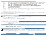
EXT:  

If EXT is SET then an IRQ has been fired from the DIO13 Secondary Function “External IRQ”.  Refer to DIO Control (+48) for de

tails on DIO Secondary Functions. 

LDAC: 

If LDAC is SET then an IRQ has been fired from the DIO12 Secondary Function “LDAC”.  Refer to DIO Control (+48) for details o

n DIO Secondary Functions. 

FOF: 

If FOF is SET then an IRQ has been fired because the ADC FIFO has Overrun: More data was acquired than fit in the ADC FIFO. 

FAF:  

If FAF is SET then an IRQ has been fired because the ADC FIFO Count (+28) has reached the configured FIFO Almost Full IRQ Threshold (+20). 

DTO: 

If DTO is SET then a DMA Timeout IRQ has been fired. 

DDONE: 

If DDONE is SET then a DMA Done IRQ has been fired. 

ADCSTART: 

If ADCSTART is SET then an IRQ has been fired from the DIO14 Secondary Function “ADCSTART”.  Refer to DIO Control (+48) for d

etails on DIO Secondary 

Functions. 

ADCTRIG: 

If ADCTRIG 

is SET then an IRQ has been fired from the DIO15 Secondary Function “ADCTRIG”. Refer to DIO Control (+48) for details on DIO 

Secondary 

Functions. 


Bits D7 through D0 indicate if the corresponding IRQ has been enabled.   

Write IRQ Status bits SET to clear the latched IRQ Status bit(s).  Typically, code will read +40 and write the value to +40 to clear all detected IRQs and leave the IRQ enables unchanged. 

Write IRQ Enable bits SET to enable corresponding IRQ sources. 


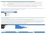
DAC Control, 4 of 32-bit Memory BAR[1]Read/Write 32-bits only 

bit  D31 through D24 

D23 through D20 

D19 through D16 

D15 through D0 

Name  UNUSED 

C3  C2 

C1 

C0 

A3  A2  A1  A0  16-bit DAC Counts (0-FFFF) 

Please refer to the LTC1664 Data Sheet for details. 

Consult the AIOAIO Software Reference, or our sample programs’ source, to avoid the hassle:


DAC_SetRange1(iBoard, iChannel, iRange); 
DAC_OutputV(iBoard, iChannel, double Voltage); 


ADC Base Clock, C of 32-bit Memory BAR[1]Read Only 32-bits only 

ADC Base Clock:  Reading this 32-bit register returns the speed (in Hertz) of the clock used to generate ADC Start Conversions.  Typical value is 125Million (125MHz), but for 

broadest compatibility software should always read this register during init, and always use the read value when calculating what, if any, divisor to write to the 
ADC Rate Divisor register. 


ADC Rate Divisor, 10 of 32-bit Memory BAR[1]Read/Write 32-bits only 

ADC Rate Divisor: Write a 32-bit divisor to the ADC Rate Divisor register to control the speed at which ADC Conversions occur in selected ADC Conversion Start Modes.  

Actual ADC Start Rate (Hz) = ADC Base Clock ÷ ADC Rate Divisor 
ADC Rate Divisor = integer(ADC Base Clock ÷ Target ADC Start Rate) 


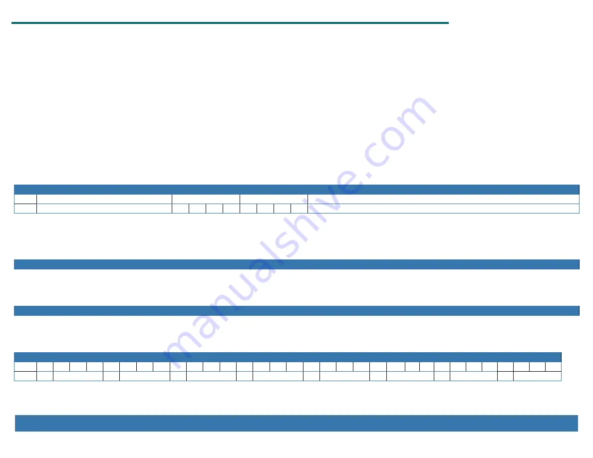
ADC Advanced Sequencer Gain Control, 18 of 32-bit Memory BAR[1]Read/Write 32-bits only 

bit  D31  D30  D29  D28  D27  D26  D25  D24  D23  D22  D21  D20  D19  D18  D17  D16  D15  D14  D13  D12  D11  D10  D9  D8  D7  D6  D5  D4  D3  D2  D1  D0 

Name  RSV  AIN 7 GAIN2:0  RSV  AIN 6 GAIN2:0  RSV  AIN 5 GAIN2:0  RSV  AIN 4 GAIN2:0  RSV  AIN 3 GAIN2:0  RSV  AIN 2 GAIN2:0  RSV  AIN 1 GAIN2:0  RSV  AIN 0 GAIN2:0 

Each nybble configures the gain of the corresponding Analog Input channel ONLY when the ADC is running in Advanced Sequenced mode. 

Summary of Contents for MPCIE-AIO16-16F Series

Page 1: ...www ACCES IO 10623 Roselle Street 800 326 1649 http acces io mPCIe AIO16 16F San Diego CA 92121 1506 USA sales accesio com MADE IN THE USA 16 ANALOG INPUT 4 ANALOG OUTPUT FOR MINI PCI EXPRESS HARDWARE MANUAL MODELS MPCIE AIO16 16F FAMILY ...

Page 2: ...ial Inputs 7 channel by channel programmable differential input ranges from 0 64V up to 24 576V Sustained sampling rates up to 1MHz 2Msps A D starts via software or periodic hardware timer Ease of use 16 bit 2MSPS complete data acquisition system High impedance 8 channel input 1 MΩ Four 16 bit analog outputs 5 per channel programmable ranges 0V to 5V 0V to 10V 2 5V 5V 10V Outputs Drive 10mA Guaran...

Page 3: ...5mm sizes Some computers may provide stand offs Please consult your computer manufacturer if it requires a different size The mPCIe standard like its PCI Mini Card predecessor was designed assuming use primarily in Laptop or Notebook and similar devices where physical dimension is often the paramount design constraint In Data Acquisition and Control applications low weight and vibration tolerance ...

Page 4: ...le in the FIFO 30 R ADC FIFO Data ADC FIFO 38 W R ADC Control ADAS3022 and ADC Control bits 44 W R DIO Data 2 bits of DIO Data 48 W R DIO Control Digital Secondary Function enable bits and direction control for each I O Group DIO 1 and DIO 0 68 R Revision FPGA code revision All these registers can be operated from any operating system using any programming language using either no driver at all ke...

Page 5: ... Write 32 bits only bit D31 through D24 D23 through D20 D19 through D16 D15 through D0 Name UNUSED C3 C2 C1 C0 A3 A2 A1 A0 16 bit DAC Counts 0 FFFF Please refer to the LTC1664 Data Sheet for details Consult the AIOAIO Software Reference or our sample programs source to avoid the hassle DAC_SetRange1 iBoard iChannel iRange DAC_OutputV iBoard iChannel double Voltage ADC Base Clock Offset C of 32 bit...

Page 6: ...ame UNUSED FAF FAF Write any 12 bit value 0 4095 to set the amount of entries in the ADC FIFO allowed to accumulate before a FIFO Almost Full IRQ is fired In Software ADC Start mode ADC Rate Divisor 10 cleared to zero the FIFO is 32 bits wide able to hold up to 4095 conversion results statuses In all other ADC Start Modes the ADC FIFO is 64 bits wide holds two ADC Conversions statuses per FIFO ent...

Page 7: ...ow to translate RAW format ADC data into Volts or skip the hassle and use our AIOAIO dll API Library ADC_GetImmediateV iBoard pVolts iChannel iRange ADC_GetImmediateScanV iBoard pVolts etc ADC Control Offset 38 of 32 bit Memory BAR 1 Read Write 32 bits only bit D31 through D19 D18 D17 D16 D15 D14 through D12 D11 D10 D9 through D7 D6 D5 D4 D3 D2 D1 D0 Name UNUSED RSV CONFIG GO RSV INx2 0 COM RSV Ga...

Page 8: ...ta BAR n Description 1 0 DMA Registers 3 2 I O Registers A NOTE ABOUT PERFORMANCE The PCI Express bus and the PCI Express Mini Card standard are capable of very high bandwidth but the latency per transaction is roughly the same as all the other busses it hasn t improved in decades This means you can expect to usually see a not less than 1MHz transaction rate Typical rates exceed 3MHz 0 3µs Unfortu...

Page 9: ...30mA from mPCIe Bus I O Interface Connectors On card Molex 501190 4017 40 pin latching Mating Molex 501189 4010 On cable Male D Sub Miniature 37 pin Mating Female D Sub Miniature 37 pin Model Options T Extended Temperature Operation 40 to 85 C I 4 20mA inputs PD Pseudo differential inputs Sxx Special configurations 10 50mA inputs input voltage dividers conformal coating etc CHAPTER 9 CERTIFICATION...

Page 10: ... give the unit model number serial number and a description of the failure symptom s We may suggest some simple tests to confirm the failure We will assign a Return Material Authorization RMA number which must appear on the outer label of the return package All units components should be properly packed for handling and returned with freight prepaid to the ACCES designated Service Center and will ...

Reviews: