SERIES IP400 INDUSTRIAL I/O PACK 40-CHANNEL DIGITAL INPUT MODULE
___________________________________________________________________________________________
-4-
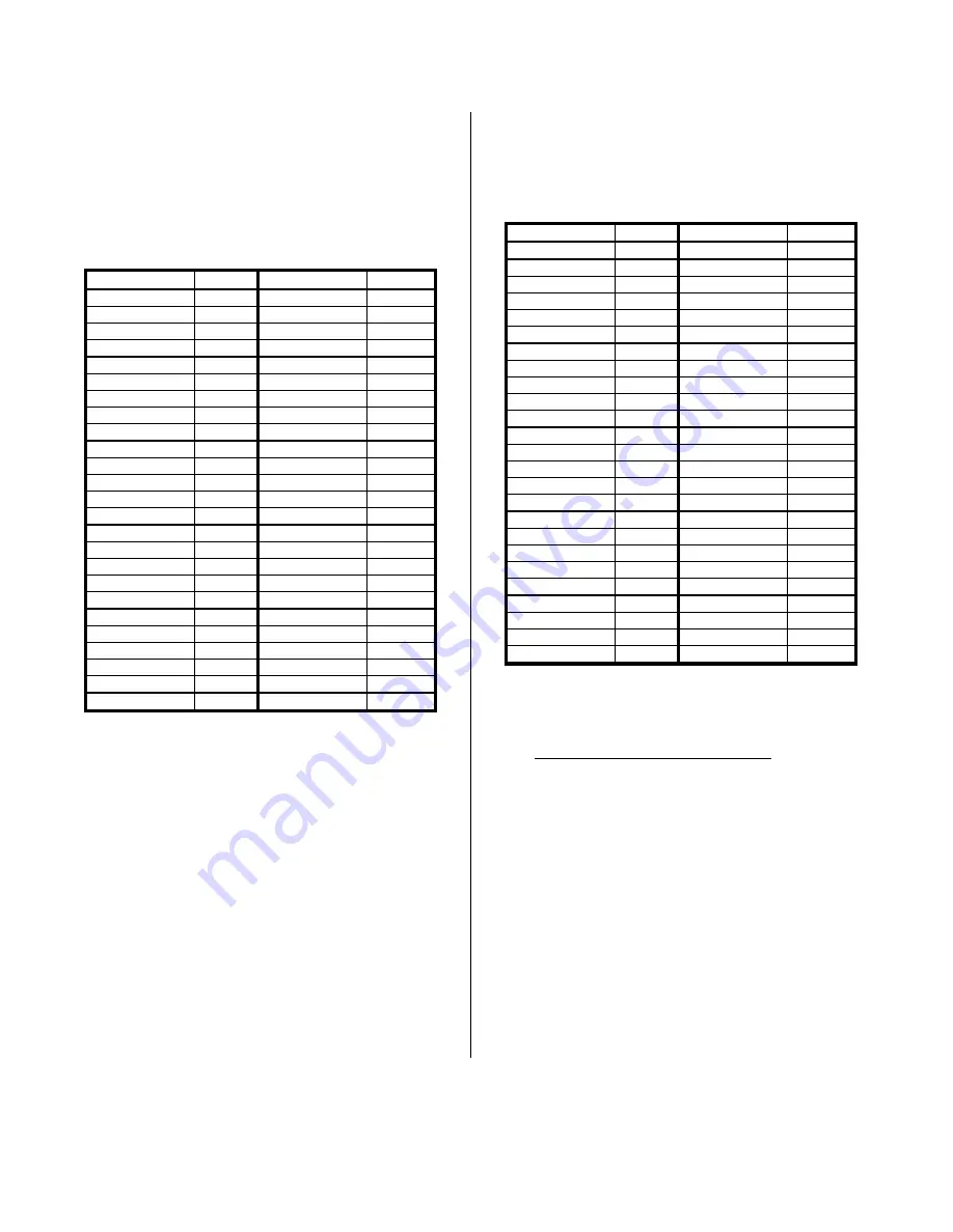
P2 pin assignments are unique to each IP model (see Table 2.1)
and normally correspond to the pin numbers of the front-panel, field
I/O interface connector on the carrier board (you should verify this
for your carrier board). The IP400 P2 connector shares the same
signal pinouts with Acromag Model IP405 40-Channel Output
Boards, making it directly compatible for “loopback” monitoring of the
IP405 output states.
Table 2.1: IP400 Field I/O Pin Connections (P2)
Pin Description
Number
Pin Description
Number
IN00
1
IN25
32
IN01
2
IN26
33
IN02
3
IN27
34
IN03
4
IN28
36
IN04
6
IN29
37
IN05
7
IN30
38
IN06
8
IN31
39
IN07
9
IN32
41
IN08
11
IN33
42
IN09
12
IN34
43
IN10
13
IN35
44
IN11
14
IN36
46
IN12
16
IN37
47
IN13
17
IN38
48
IN14
18
IN39
49
IN15
19
COMMON
5
IN16
21
COMMON
10
IN17
22
COMMON
15
IN18
23
COMMON
20
IN19
24
COMMON
25
IN20
26
COMMON
30
IN21
27
COMMON
35
IN22
28
COMMON
40
IN23
29
COMMON
45
IN24
31
COMMON
50
Input Noise and Grounding Considerations
This model is non-isolated between the logic and field input
grounds since input common is electrically connected to the IP
module ground. Consequently, the field I/O connections are not
isolated from the carrier board and backplane. Care should be taken
in designing installations without isolation to avoid noise pickup and
ground loops caused by multiple ground connections. Refer to
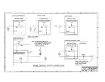
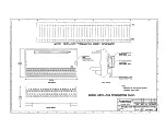
Drawing 4501-518 for example input and grounding connections.
IP Logic Interface Connector (P1)
P1 of the IP module provides the logic interface to the mating
connector on the carrier board. This connector is a 50-pin female
receptacle header (AMP 173279-3 or equivalent) which mates to the
male connector of the carrier board (AMP 173280-3 or equivalent).
This provides excellent connection integrity and utilizes gold-plating
in the mating area. Threaded metric M2 screws and spacers are
supplied with the IP module to provide additional stability for harsh
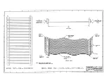
environments (see Drawing 4501-434 for assembly details). Field
and logic side connectors are keyed to avoid incorrect assembly.
The pin assignments of P1 are standard for all IP modules
according to the Industrial I/O Pack Specification (see Table 2.2).
Note that the IP400 does not utilize all of the logic signals defined for
the P1 connector and these are indicated in BOLD ITALICS.
Table 2.2: Standard Logic Interface Connections (P1)
Pin Description
Number
Pin Description
Number
GND
1
GND
26
CLK
2
+5V
27
Reset*
3
R/W*
28
D00
4
IDSEL*
29
D01
5
DMAReq0*
30
D02
6
MEMSEL*
31
D03
7
DMAReq1*
32
D04
8
IntSel*
33
D05
9
DMAck0*
34
D06
10
IOSEL*
35
D07
11
RESERVED
36
D08
12
A1
37
D09
13
DMAEnd*
38
D10
14
A2
39
D11
15
ERROR*
40
D12
16
A3
41
D13
17
INTReq0*
42
D14
18
A4
43
D15
19
INTReq1*
44
BS0*
20
A5
45
BS1*
21
STROBE*
46
-12V
22
A6
47
+12V
23
ACK*
48
+5V
24
RESERVED
49
GND
25
GND
50
Asterisk (*) is used to indicate an active-low signal.
BOLD ITALIC Logic Lines are NOT USED by this IP Model.
3.0 PROGRAMMING INFORMATION
ADDRESS MAPS
This board is addressable in the Industrial Pack I/O space to
control the acquisition of digital inputs from the field. The I/O space
may be as large as 64, 16-bit words (128 bytes) using address lines
A1..A6, but the IP400 only uses a portion of this space. The I/O
space address map for the IP400 is shown in Table 3.1. Note the
base address for the IP module I/O space (see your carrier board
instructions) must be added to the addresses shown to properly
access the I/O space. Accesses can be performed on an 8-bit
(D08[EO]), or 16-bit word (D16) basis.


