SERIES IP400 INDUSTRIAL I/O PACK 40-CHANNEL DIGITAL INPUT MODULE
___________________________________________________________________________________________
-5-
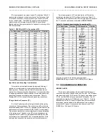
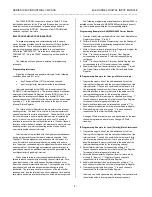
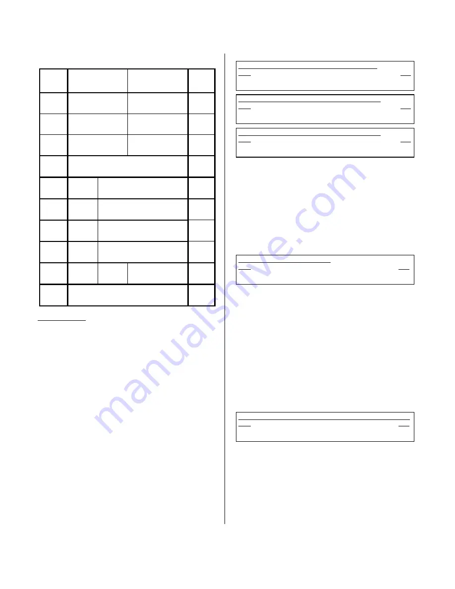
Table 3.1: IP400 I/O Space Address (Hex) Memory Map
4
EVEN
Base
Addr.+
EVEN Byte
D15 D08
ODD Byte
D07 D00
ODD
Base
Addr.+
00
READ- Digital Input
Channel Register A
CH15
↔
CH08
READ- Digital Input
Channel Register A
CH07
↔
CH00
01
02
READ- Digital Input
Channel Register B
CH31
↔
CH24
READ- Digital Input
Channel Register B
CH23
↔
CH16
03
04
(FF)
Not Driven
1
READ- Digital Input
Channel Register C
CH39
↔
CH32
05
06
(0FFF)
NOT USED
3
07
08
Driven
LOW
2
15.....12
R/W - Interrupt Enable
Register
2
CH11
↔
CH00
09
0A
Driven
LOW
2
15.....12
R/W -Interrupt Type Config.
Register
2
CH11
↔
CH00
0B
0C
Driven
2
LOW
15.....12
R/W - Interrupt Polarity
Register
2
CH11
↔
CH00
0D
0E
Driven
2
LOW
15.....12
R/W - Interrupt Status Register
2
CH11
↔
CH00
0F
10
Driven
2
LOW
15.....12
(F)
Driven
HIGH
R/W - Interrupt
Vector Register
1
11
12
↓↓↓↓
7E
(0FFF)
NOT USED
3
13
↓↓↓↓
7F
Notes (Table 3.1):
1. These bits of this register are not driven. Pull-ups on the carrier
board data bus will cause these bits to always read High (1’s).
2. The upper 4 bits of these 16-bit registers are driven low (0’s).
3. These registers have no function. The upper 4 bits of these 16-
bit registers are driven low (0’s) and pullups on the data bus will
cause the lower 12-bits to read high (1’s). Embedded “Not
Used” addresses occur due to the IP400’s use of the same
register architecture as Acromag Model IP408.
4. All Read and Write operations require 1 wait state.
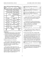
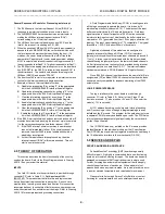
IP Digital Input Registers A, B, & C (Read Only)
When the Digital Input Channel Data Registers are read, the
value read corresponds to the actual state of the input channels at
the time of the read. A “0” bit means that the corresponding input
signal is below TTL threshold, a “1” bit means that the
corresponding input signal is at or above the TTL threshold
(approximately 1.6V, typical).
40 Input channels numbered 0 through 39 may be read.
Channel Read operations use 8-bit (D08[EO]), or 16-bit (D16) words
with the lower ordered bits corresponding to the lower-numbered
channels for the register of interest (see below). Register A
monitors input channels 0 through 15. Register B monitors input
channels 16 through 31. Register C monitors input channels 32
through 39. Pullups on the carrier board data bus will cause the
upper 8 bits of Register C to read back as high (1’s).
REGISTER A (INPUT CHANNELS 0 THROUGH 15):
MSB _ _ _ _ _ _ _ _ _ _ _ _ _ _ LSB
15 14 13 12 11 10 9 8 7 6 5 4 3 2 1 0
CH15...................................CH8 CH7.....................................CH0
REGISTER B (INPUT CHANNELS 16 THROUGH 31):
MSB _ _ _ _ _ _ _ _ _ _ _ _ _ _ LSB
15 14 13 12 11 10 9 8 7 6 5 4 3 2 1 0
CH31.................................CH24 CH23...................................CH16
REGISTER C (INPUT CHANNELS 32 THROUGH 39):
MSB _ _ _ _ _ _ _ _ _ _ _ _ _ _ LSB
15 14 13 12 11 10 9 8 7 6 5 4 3 2 1 0
1 1 1 1 1 1 1 1 CH39...................................CH32
It is recommended that unused input points not be left floating,
but pulled high or low. The unused upper 8 bits of Register C are
“Don’t Care” and will always read high (1’s) for D16 accesses.
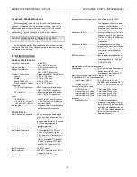
Interrupt Enable Register (R/W)
The digital input channel Interrupt Enable Register provides a
mask bit for each of the 12 possible interrupt channels (channels 0-
11 only). A “0” bit will prevent the corresponding input channel from
generating an external interrupt. A “1” bit will allow the
corresponding input channel to generate an interrupt.
INTERRUPT ENABLE REGISTER:
MSB _ _ _ _ _ _ _ _ _ _ _ _ _ _ LSB
15 14 13 12 11 10 9 8 7 6 5 4 3 2 1 0
0 0 0 0 CH11...............................................................CH0
All input channel interrupts are masked (“0”) following a reset.
The unused upper 4 bits of this 16-bit register are always driven low
(0’s) for D08(E) or D16 accesses.
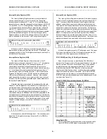
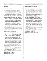
Interrupt Type Configuration (COS or H/L) Register (R/W)
The Interrupt Type Configuration Register determines the type
of input channel transition that will generate an interrupt for each of
the 12 possible interrupt channels (channels 0-11 only). A “0” bit
means that an interrupt will be generated when the input channel
level specified by the Interrupt Polarity Register occurs (i.e. Low or
High level transition interrupt). A “1” bit means the interrupt will
occur when a Change-of-State (COS) occurs at the corresponding
input channel (i.e. any state transition). Note that interrupts will not
occur unless they are enabled (see the Interrupt Enable Register).
INTERRUPT TYPE (COS or H/L) CONFIGURATION REGISTER:
MSB _ _ _ _ _ _ _ _ _ _ _ _ _ _ LSB
15 14 13 12 11 10 9 8 7 6 5 4 3 2 1 0
0 0 0 0 CH11...............................................................CH0
All bits are set to “0” following a reset which means that the
inputs will cause interrupts for the levels specified by the digital input
channel Interrupt Polarity Register. The unused upper 4 bits of this
16-bit register are always driven low (0’s) for D08(E) or D16
accesses.


