

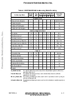
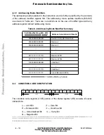
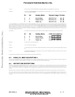


MOTOROLA
DSP56000/DSP56001 USER’S MANUAL
A - 1
APPENDIX A
INSTRUCTION SET DETAILS
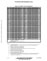
This appendix contains detailed information about each instruction in the DSP56000/
DSP56001 instruction set. An instruction guide is presented first to help understand the
individual instruction descriptions. This guide is followed by sections on notation and
addressing modes. Since parallel moves are allowed with many of the instructions, they
are discussed before the instructions. The instructions are then discussed in alphabetical
order.
A.1
INSTRUCTION GUIDE
The following information is included in each instruction description with the goal of mak-
ing each description self-contained:
1.
Name and Mnemonic:
The mnemonic is highlighted in
bold
type for easy refer-
ence.
2.
Assembler Syntax and Operation:
For each instruction syntax, the corresponding
operation is symbolically described. If there are several operations indicated on a
single line in the operation field, those operations do not necessarily occur in the
order shown but are generally assumed to occur in parallel. If a parallel data move
is allowed, it will be indicated in parenthesis in both the assembler syntax and oper-
ation fields. If a letter in the mnemonic is optional, it will be shown in parenthesis in
the assembler syntax field.
3.
Description:
A complete text description of the instruction is given together with
any special cases and/or condition code anomalies of which the user should be
aware when using that instruction.
4.
Example:
An example of the use of the instruction is given. The example is shown
in DSP56000/DSP56001 assembler source code format. Most arithmetic and logi-
cal instruction examples include one or two parallel data moves to illustrate the
many types of parallel moves that are possible. The example includes a complete
explanation, which discusses the contents of the registers referenced by the
instruction (but not those referenced by the parallel moves) both before and after
the execution of the instruction. Most examples are designed to be easily under-
stood without the use of a calculator.
5.
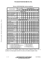
Condition Codes:
The status register is depicted with the condition code bits which
can be affected by the instruction highlighted in
bold
type. Not all bits in the status
register are used. Those which are reserved are indicated with a double asterisk
and are read as zeros.
6.
Instruction Format:
The instruction fields, the instruction opcode, and the instruc-
tion extension word are specified for each instruction syntax. When the extension
F
re
e
sc
a
le
S
e
m
ic
o
n
d
u
c
to
r,
I
Freescale Semiconductor, Inc.
For More Information On This Product,
Go to: www.freescale.com
n
c
.
..