background image

PRELIMINARY ISD1700 SERIES   


         Publication Release Date: Nov 6, 2008      


- 41 - 


Revision 1.31 

Before starting to write the program code, one has to fully understand the definition of each command 
and how to implement each of them correctly. If not, you may end up to spend lots of time and efforts 
in debugging the program code. The following several sections illustrate exactly how the 
communication sequence of each SPI command should be. Bear in mind that the first bit of each input 
data byte shifting into the MOSI must be LSB, whereas the first bit of data byte coming out from the 
MISO is LSB. Also, care must be provided to fulfill the initial conditions on the 

SS

, SCLK and MOSI 

inputs (as shown in Section 10.2). If wrong format is sent, then the device may not response at all or 
may respond strangely. Also, not every command will generate an interrupt feedback signal to the 
host in responding to the operation requested. Thus, precautions must be well considered to ensure 
that the device is ready to accept a new instruction. Otherwise, the instruction sent will be ignored.   
 

11.1  SPI


P

RIORITY 

C

OMMANDS


This class of SPI commands will always be accepted by the ISD1700. They control power up and 
down of the device, interrogating the status of the device and clearing interrupt requests. 

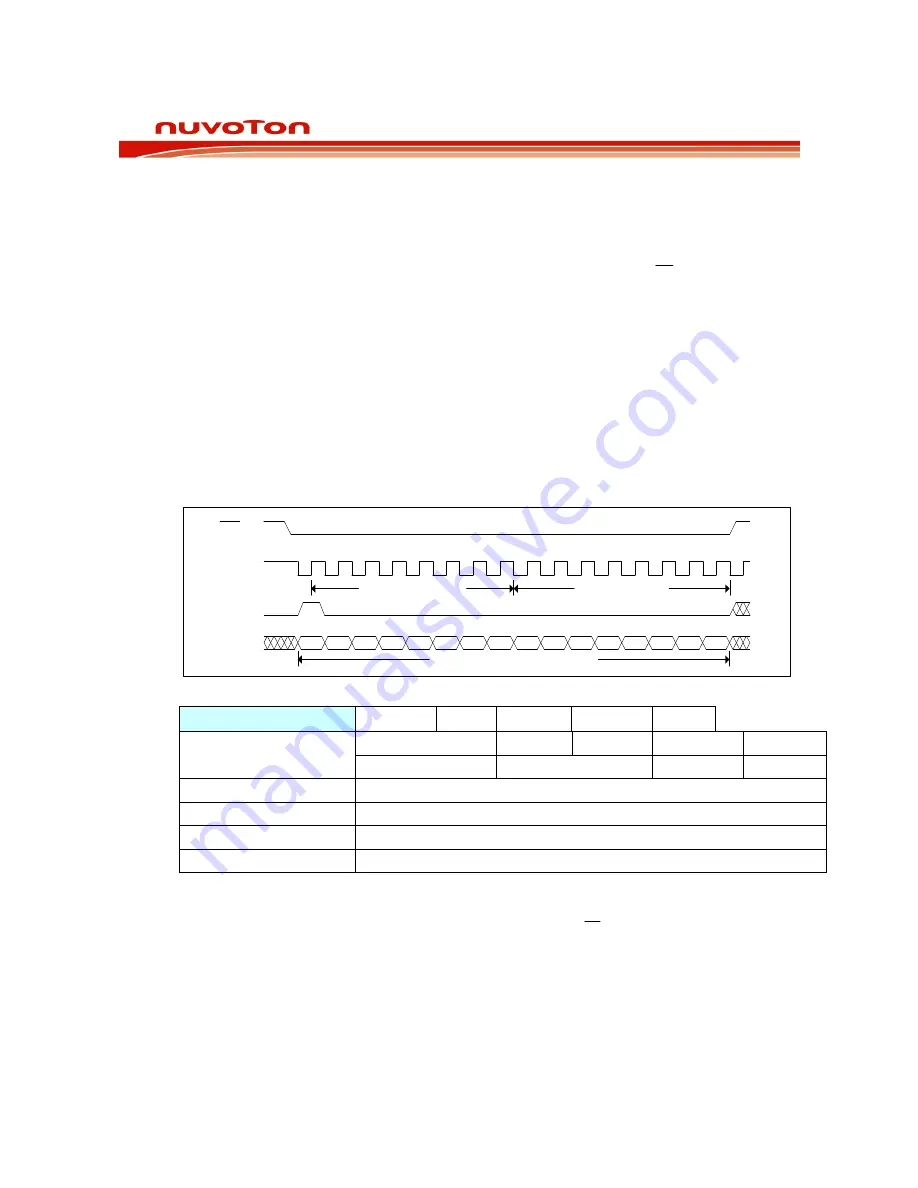
11.1.1 PU (0x01) Power Up 

B0 B1 B2 B3 B4 B5 B6 B7 B8 B9 B10 B11 B12 B13 B14 B15

SCLK

MOSI

MISO

SS

Data Byte 1

Command (01h)

LSB

MSB

0

1

2

3

4

5

6

7

8

9

10

11

12

13

14

15

LSB

MSB

Status Register 0 : Bytes #1 & #2


PU 

Opcode: 0x01  0x00 

Interrupt: No 

Byte Sequence: 

MOSI 

0x01   

0x00 


MISO SR0 


Description: Power 

up 


State before Execution 

Power Down 

State after Execution 

Idle/FT 

Registers Affected 

SR0: PU bit, SR1: RDY bit   

This command wakes up the ISD1700 device and enables it into the idle state. Upon 
executing this command, PU bit of SR0 and RDY bit of SR1 are set to 1. This command does 
not generate an interrupt. Once in SPI mode, the input from 

FT

pin is ignored and its function 

is replaced by Bit 6 of the APC register. SPI mode is exited via a PD (power down) 
command. 

Summary of Contents for ISD1700 series

Page 1: ...PRELIMINARY ISD1700 SERIES Publication Release Date Nov 6 2008 1 Revision 1 31 ISD1700 Series Design Guide...

Page 2: ...Push Button Mode 16 6 3 2 SPI Mode 16 7 ANALOG PATH CONFIGURATION APC 17 7 1 APC Register 17 7 2 Device Analog Path Configurations 18 8 STANDALONE PUSH BUTTON OPERATIONS 19 8 1 Sound Effect SE Mode 19...

Page 3: ...ng from SPI mode to Standalone Mode 35 10 5 ISD1700 Device Registers 35 10 5 1Status Register 0 SR0 35 10 5 2Status Register 1 SR1 37 10 5 3APC Register 37 10 5 4Playback Pointer PLAY_PTR 38 10 5 5Rec...

Page 4: ...6 General Guidelines for Writing Program Code 58 11 7 Examples of Various Operating Sequences 59 11 7 1Record Stop and Playback operations 60 11 7 2SetRec and SetPlay operations 61 11 7 3Wr_APC2 SetR...

Page 5: ...PRELIMINARY ISD1700 SERIES Publication Release Date Nov 6 2008 5 Revision 1 31 15 TYPICAL APPLICATION CIRCUITS 76 15 1 Good Audio Design Practices 79 16 ORDERING INFORMATION 80 17 VERSION HISTORY 81...

Page 6: ...rt Record Stop Record Erase Forward Global Erase and etc Recordings are stored into on chip Flash memory providing zero power message storage This unique single chip solution is made possible through...

Page 7: ...Es for audible indication o Optional vAlert voiceAlert to indicate the presence of new messages o LED stay on during recording blink during playback forward and erase operations y Dual operating modes...

Page 8: ...ulti Level Storage Array Power Conditioning Automatic Gain Control Anti Aliasing Filter Smoothing Filter Sampling Clock SP SP AGC MIC MIC ROSC VCCA AUD AUX Amp SPI Interface VCCD Device Control VSSD V...

Page 9: ...22 MIC MIC VCCA 21 SP ERASE 1 2 3 4 5 6 7 8 9 10 11 12 13 14 20 19 18 17 16 15 REC MOSI SS SCLK MISO AnaIn VSSP2 VCCP VSSP1 Sp AUD AUX AGC VOL ROSC VSSD TSOP ISD1700 VSSA MIC MIC SP 1 2 3 4 5 6 7 8 9...

Page 10: ...Slave Select This input when low selects the device as slave device and enables the SPI interface This pin has an internal pull up resistor 1 VSSA 8 1 Analog Ground It is important to have a separate...

Page 11: ...put whereas AUX is a single ended voltage output They can be used to drive an external amplifier The factory default is set to AUD This output can be powered down by D9 of APC register The factory def...

Page 12: ...cord The device starts recording whenever REC switches from High to Low and stays at Low Recording stops when the signal returns to High This pin has an internal pull up device 1 and an internal debou...

Page 13: ...n 1 31 PIN NAME PDIP SOIC TSOP FUNCTIONS 3 VSSD 28 21 Digital Ground It is important to have a separate path for each ground signal including VSSA VSSD VSSP1 and VSSP2 to minimize the noise coupling N...

Page 14: ...7 secs 362 secs 4 kHz 60 secs 80 secs 100 secs 120 secs 180 secs 240 secs 300 secs 360 secs 420 secs 480 secs 6 1 3 Flash Storage The ISD1700 devices utilize embedded Flash memory to provide non volat...

Page 15: ...7210 ISD17240 Maximum Address 0x0FF 0x14F 0x19F 0x1EF 0x2DF 0x3CF 0x4BF 0x5AF 0x69F 0x78F Below figure shows the memory array architecture for ISD1700 series 000 003 SE1 004 007 SE2 008 00B SE3 00C 00...

Page 16: ...3 2 SPI Mode In SPI mode control of the device is achieved through the 4 wire serial interface Commands similar to the push button controls such as REC PLAY FT FWD ERASE VOL and RESET can be executed...

Page 17: ...cording through the MIC inputs FT via AnaIn input playback from MLS SE editing feature enabled maximum volume level active PWM driver and AUD current outputs One can use SPI commands to modify the APC...

Page 18: ...nd Address 0 Off 7 2 DEVICE ANALOG PATH CONFIGURATIONS Table 7 2 demonstrates the possible analog path configurations with ISD1700 The device can be in power down power up recording playback and or fe...

Page 19: ...e for SE2 and so forth It is crucial to recognize that the LED flashes accordingly regardless the SEs are programmed or not When none of them is programmed the blinking periods of SE1 SE2 SE3 and SE4...

Page 20: ...equency selected and illustrated in below table Table 8 1 Sound Effect Duration vs Sampling Frequency Sampling Frequency 12 kHz 8 kHz 6 4 kHz 5 3 kHz 4 kHz Duration of SE 0 33 sec 0 5 sec 0 625 sec 0...

Page 21: ...ring recording process the circular memory architecture will be destroyed As a result next time when a push button operation starts the LED will blink seven times which indicates that something unusua...

Page 22: ...TLS1 due to forward action As after the last message device flashes LED twice with blinking period TLS2 If both SE1 and SE2 are programmed after playing a message except the last one device plays SE1...

Page 23: ...twice The LED blinking period is determined by the recorded duration TSE2 of SE2 Playback the first message The LED flashes during this entire process Triggering of the FWD operation during an erase o...

Page 24: ...differently according to the current condition of the device If SEs are not programmed o The device will blink LED twice with blinking period TLS2 once ERASE is triggered to indicate the current mess...

Page 25: ...ill delete the current played message if it is the first or last one Figure 8 1 Global Erase Operation 8 2 5 Reset Operation recommended to connect th RESET to ground which should satisfy the requirem...

Page 26: ...UD outputs when the de to vice is idle During recording device will record the FT 8 3 VALE If this optional feature is enabled after a recording operation the LED output will blink once every few seco...

Page 27: ...AIN INPUT AMPLIFIER Ra Ra Fcutoff 1 2 pi Ra Ccoup 42K 42K Figure 8 3 AnaIn input impedance When the device is powered up 8 5 SYSTEM MANAGEMENT While in Standalone mode it is recommended the designer t...

Page 28: ...er to address 0x010 To comply with the circular memory architecture all messages must form a contiguous block with no empty space between them and there must be at least one blank row left between the...

Page 29: ...sequent REC command will record message 1 Now the playback pointer will point to the beginning of message 1 and the record pointer to the next row after message 1 Three more recordings will write mess...

Page 30: ...will wrap the playback pointer to message four the second message in the circular queue Now if we record until the memory is full the record pointer becomes invalid and no further record commands wil...

Page 31: ...the rising edge of the SCLK signal and clocked out of the MISO pin on the falling edge of the SCLK signal with LSB first 4 The opcodes contain command data and address bytes depending upon the command...

Page 32: ...e Data Byte2 Start Address Byte1 LSB Bit 23 Bit 22 Bit 21 Bit 20 Bit 19 Bit 18 Bit 17 Bit 16 X S7 X S6 X S5 X S4 D11 S3 D10 S2 D9 S1 D8 S0 MSB 4 th Byte Data Byte3 Start Address Byte2 LSB Bit 31 Bit 3...

Page 33: ...w Byte MSB Bit 16 Bit 17 Bit 18 Bit 19 Bit 20 Bit 21 Bit 22 Bit 23 D0 CMD_ Err D1 Memory Full D2 Power Up D3 EOM D4 Interrupt D5 A0 D6 A1 D7 A2 LSB 4 th Byte Data Byte 2 or SR0 High Byte MSB Bit 24 Bi...

Page 34: ...ds o Accepted at any time and do not require state machine intervention o PU STOP PD RD_STATUS CLR_INT DEVID RESET Circular memory commands o Execute operations similar to in Standalone mode o PLAY RE...

Page 35: ...ayback Instead the device continues to execute the 2nd SET_PLAY command As a result the chip will playback the second message This action will minimize any potential dead time between two recorded mes...

Page 36: ...an EOM is detected It can be cleared by CLR_INT command 2 PU This bit is set to 1 when the device is powered up and operating in SPI mode 1 FULL This bit when set to 1 indicates memory array is full...

Page 37: ...ding 2 PLAY This bit 1 indicates current operation is playback 1 ERASE This bit 1 indicates current operation is erase 0 RDY In standalone mode RDY 1 indicates the device is ready to accept command In...

Page 38: ...escription Pointer at first available row in the memory Access Read RD_REC_PTR Changed by REC 10 5 6 DEVICEID Register DEVICEID Size 8 bits Type Read Bit Sequence D7 D6 D5 D4 D3 D2 D1 D0 CHIPID Reserv...

Page 39: ...1 st 2 bytes and operating status in 3rd byte RD_PLAY_PTR 0x06 0x00 0x00 0x00 Returns status bits current row counter in 1st 2 bytes and playback pointer in 3rd 4 th bytes PD 0x07 0x00 Power down the...

Page 40: ...rt address of next message Forward will be ignored during operating except Play CHK_MEM 0x49 0x00 Check circular memory EXTCLK 0x4A 0x00 Enable disable external clock mode SET_PLAY 0x80 0x00 S7 S0 xxx...

Page 41: ...us precautions must be well considered to ensure that the device is ready to accept a new instruction Otherwise the instruction sent will be ignored 11 1 SPI PRIORITY COMMANDS This class of SPI comman...

Page 42: ...This command stops the current operation and returns the device back to the state prior to the operation This command is only valid for the PLAY REC SET_PLAY and SET_REC operations Upon completion an...

Page 43: ...CLR_INT Opcode 0x04 0x00 Interrupt No Byte Sequence MOSI 0x04 0x00 MISO SR0 Description Read Status and Clear INT and EOM State before Execution Any State after Execution Does not affect state clears...

Page 44: ...E2 SE3 Status Register 0 Status Bits 1st Byte 2nd Byte 3rd Byte Status Bits Current Row Address Bits Status Register 1 0 1 2 3 4 5 6 7 PU EOM INT A0 A2 0 1 2 3 4 5 6 7 0 1 2 3 4 5 6 7 A3 A10 Figure 11...

Page 45: ...None The Read Device ID command reads the ID register and returns the device name in the third byte of MISO to identify which device is present See Table 10 5 for a description of DEVICEID register b...

Page 46: ...RDY bits The PLAY command starts playback operation from current message and stops when it reaches EOM or receives STOP command During playback the device only responds to STOP RESET CLR_INT RD_STATUS...

Page 47: ...1 Command 42h LSB MSB 0 1 2 3 4 5 6 7 8 9 10 11 12 13 14 15 MSB LSB Status Register 0 Bytes 1 2 ERASE Opcode 0x42 0x00 Interrupt Yes Byte Sequence MOSI 0x42 0x00 MISO SR0 Description Device will delet...

Page 48: ...The G_ERASE command deletes all messages within the entire memory array except the SE portion rows 0x000 0x00F regardless the location of the PLAY_PTR In the G_ERASE mode the device only responds to R...

Page 49: ...B LSB Status Register 0 Bytes 1 2 CHK_MEM Opcode 0x49 0x00 Interrupt Yes Byte Sequence MOSI 0x49 0x00 MISO SR0 Description Check the validity of circular memory architecture State before Execution Idl...

Page 50: ...sters Affected None This command reads out the playback pointer address where a push button compatible playback or PLAY starts from Prior sending this command ensure circular memory architecture is sa...

Page 51: ...MOSI MISO SS MSB LSB MSB LSB Status Register 0 Bytes 1 2 APC Register A11 A0 RD_APC Opcode 0x44 0x00 0x00 0x00 Interrupt No Byte Sequence MOSI 0x44 0x00 0x00 0x00 MISO SR0 APC 7 0 xxxxx APC 11 8 Descr...

Page 52: ...B Data Byte 2 LSB B0 B1 B2 B3 B4 B5 B6 B7 B8 B9 B10 B11 B12 B13 B14 B15 B16 B17 B18 B19 B20 B21 B22 B23 SCLK MOSI MISO SS 0 1 2 3 4 5 6 7 8 9 10 11 12 13 14 15 16 17 18 19 20 21 22 23 D0 D1 D2 D3 D4 D...

Page 53: ...egister This value is loaded from NVCFG register to the APC register after a power on condition or RESET The CMD_ERR bit of SR0 is set if ISD1700 is not in idle state when this command is sent 11 3 5...

Page 54: ...us precautions must be paid to address to the beginning of the memory Also care must be taken in accessing the SE rows 0x000 0x00F and SEs should be handled independently 11 4 1 SET PLAY 0x80 SCLK MOS...

Page 55: ...es smoothly 11 4 2 SET_REC 0x81 SCLK MOSI MISO SS 0 1 2 3 4 5 6 7 8 9 10 11 12 13 14 15 16 17 18 19 20 Data Byte 1 Command 81h Start Address 16 bits LSB B0 B1 B2 B3 B4 B5 B6 B7 B8 B9 B10 B11 B12 B13 B...

Page 56: ...2 S3 S4 MSB B22 B23 S6 S7 B24 B25 B26 B27 B28 B29 B30 B31 S8 S9 S10 S5 B21 X X X X X Status Register 0 Bytes 1 2 Status Register 0 Bytes 1 2 32 33 34 35 36 37 38 39 40 41 42 43 44 45 46 47 48 49 50 51...

Page 57: ...tor of the device is disabled Instead an external clock is required to apply to the Rosc pin and the external resistor at Rosc pin must be removed When XCLK mode is disabled then the external clock si...

Page 58: ...n all the operations is a good habit because this will provide a direct visual illustration to the end user such as LED on during recording or LED blinking during playback if LED is connected appropri...

Page 59: ...or that number Due to the uncontrollable external factors the approach of utilizing delay is not recommended unless additional buffer on the delay is factored in Rule 6 Set initial SPI condition as li...

Page 60: ...Record Stop and Playback operations Apply Power Reset Send PU Check CMD_ERR Monitor INT status for Completion Is CMD_ERR bit set Y N Y N Send Record Send Stop Wait Record Duration Send Play Monitor IN...

Page 61: ...tPlay operations Apply Power Reset Send PU Check CMD_ERR Monitor INT tatus for Completion s Is CMD_ERR bit set Y N Y N Send SetErase Send SetPlay Monitor INT tatus for Completion s Wait TPUD Clr_Int P...

Page 62: ...1 7 3 Wr_APC2 SetRec and SetPlay operations Apply Power Reset Send PU Check CMD_ERR Monitor INT status for Completion Is CMD_ERR bit set Y N Y N Send Wr_APC2 Send SetPlay Monitor INT status for Comple...

Page 63: ...status for Msg 1 Completion Wait TPUD Clr_Int PD Check RDY bit N Y Device Ready N Y Note Utilizing 3 consecutive SetPlay on 3 individual messages as shown then these 3 messages will be played back se...

Page 64: ...le The LED and optional SE indications include automatically in certain operations under Standalone mode but not under the SPI mode 12 1 RECORD OPERATION Tr Tf RDY TDeb REC TER TSc1 TRU TRD TSet1 Mic...

Page 65: ...evision 1 31 12 2 PLAYBACK OPERATION RDY PLAY Sp Sp TDeb TSc1 TRD Tr TSc2 TRU TLH Tf LED TCyc TDeb Figure 12 3 Playback Operation for entire message RDY Sp Sp PLAY TDeb TSc1 TSet1 Tr TSc2 TRU TLH Tf L...

Page 66: ...ision 1 31 12 3 ERASE OPERATION ERASE RDY TDeb TSc1 TRD Tr Tf LED TSc2 TLS2 TSc2 TE TDeb Figure 12 5 Single Erase Operation with No Sound Effect Sp Sp ERASE Tr Tf RDY TDeb TRD TSc1 TSc2 TRU TSE2 TRD L...

Page 67: ...67 Revision 1 31 12 4 FORWARD OPERATION FWD RDY TDeb TSc1 TRD Tr Tf LED TSc2 TLS1 or TLS2 TDeb Figure 12 7 Forward Operation with No Sound Effect FWD Tr Tf Sp Sp RDY TDeb TRD TSc1 TSc2 TRU TSE1 or TSE...

Page 68: ...SEs are recorded then Sp will have output ERASE RDY TDeb TSc1 TRD Tr Tf LED TGE1 or TE TLS2 or TSE2 TSc2 TGE2 3x TLS1 or TSE1 TLS4 or TSE4 Figure 12 9 Global Erase Operation with or without Sound Effe...

Page 69: ...TRU 2nd Message After 2nd Message starts playback If SE1 recorded Figure 12 11 Playback Two Consecutive messages RDY PLAY Sp Sp TDeb TSc1 TRD Tr Tf LED Looping playback of 2 consecutive messages until...

Page 70: ...then Sp will have output ERASE RDY TDeb TSc1 TRD Tr Tf LED TLErr TGE2 3x TLS1 or TSE1 TLS4 or TSE4 TGE1 Figure 12 13 Global Erase Operation to recover a broken circular memory architecture 12 9 PLAYB...

Page 71: ...N TYP MAX UNITS SS Setup Time TSSS 500 nsec SS Hold Time TSSH 500 nsec Data in Setup Time TDIS 200 nsec Data in Hold Time TDIH 200 nsec Output Delay TPD 500 nsec Output Delay to HighZ TDF 500 nsec SS...

Page 72: ...V to 7 0V ABSOLUTE MAXIMUM RATINGS PACKAGED PARTS 1 Condition Value Junction temperature 1500 C Storage temperature range 650 C to 1500 C Voltage Applied to any pins VSS 0 3V to VCC 0 3V Voltage appli...

Page 73: ...to 5 5 V Ground voltage VSS 2 0 V Input voltage VCC 1 0 V to 5 5 V Voltage applied to any pins VSS 0 3 V to VCC 0 3 V OPERATING CONDITIONS PACKAGED PARTS CONDITIONS VALUES Operating temperature range...

Page 74: ...in from MIC to SP AMSP 6 40 dB VIN 15 300 mV AGC 4 7 F VCC 2 4V 5 5V Speaker Output Load RSPK 8 Across both Speaker pins AUX Output Load RAux 5 k When active Speaker Output Power Pout 670 mW VDD 5 5 V...

Page 75: ...Time for SE4 TLS4 15 5K FS sec SE4 not recorded 5 SE1 Recorded Duration TSE1 4K FS sec 4 5 SE2 Recorded Duration TSE2 4K FS sec 4 5 SE3 Recorded Duration TSE3 4K FS sec 4 5 SE4 Recorded Duration TSE4...

Page 76: ...Please refer to the applications notes or consult Nuvoton for layout advice It is important to have a separate path for each ground and power back to the related terminals to minimize the noise Also...

Page 77: ...11 20 18 22 9 7 6 5 4 At 8kHz sampling freq Rosc 80 K Rosc 4 7 F FT 0 1 F Digital ground Analog ground Ground for SP Ground for SP 3 RESET 0 1 F Reset Vcc Gnd VCCA SP AUD AUX VSSD VCCD VCCA 0 1 F LED...

Page 78: ...8 22 9 7 6 5 4 At 8kHz sampling freq Rosc 80 K Rosc 4 7 F FT 0 1 F To uC SPI Digital ground Analog ground Ground for SP Ground for SP Vcc Gnd VCCA SP AUD AUX VSSD VCCD VCCA 0 1 F LED 1 K VCCD D1 2 1 2...

Page 79: ...See recommendations from below links or other Application Notes in our websites Design Considerations for ISD1700 Family AN CC1002 Design Considerations for ISD1700 Family Good Audio Design Practices...

Page 80: ...voton s worldwide web site at http www Nuvoton usa com Product Series 17 700 1 Duration 30 20 60 secs 40 26 80 secs 50 33 100 secs 60 40 120 secs 90 60 180 secs 120 80 240 secs 150 100 300 secs 180 12...

Page 81: ...ORY VERSION DATE DESCRIPTION 0 October 2006 Initial version 1 January 2007 Revise Rosc resistor value and standby current parameter Update read status command description figure 1 1 May 2007 Update th...

Page 82: ...e Copyright 2005 Nuvoton Electronics Corporation All rights reserved ChipCorder and ISD are trademarks of Nuvoton Electronics Corporation SuperFlash is the trademark of Silicon Storage Technology Inc...

Reviews: