background image

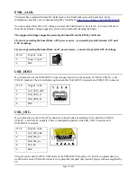
PWR_JACK

The board has a standard Olimex DC barrel jack with 2.0mm inner pin and 6.3mm hole. More 
information about the exact component might be found here: 

https://www.olimex.com/wiki/PWRJACK

You can supply either DC or AC voltage to power the board however be careful – if you provide more 
than the maximum voltage suggested, you would permanently damage the board.

The suggested voltage ranges for powering the board from the PWR_JACK are:

If you are powering the board from a DC power source – you need to provide between 6.5V and 
9.0V of voltage.

If you are powering the board from an AC power source – you need to provide 6.0V of voltage.

Pin #

Signal name

1

Power input

2

GND

USB_HOST

If you intend to use the USB_HOST connector pay attention to the position of VBUS, USB_D+, and 
USB_D- jumpers. There is multiplexing between the USB_HOST connector and USB_OTG connector.

Pin #

Signal name

1

+5V_HOST_PWR

2

USB_HOST_D-

3

USB

4

GND

USB_OTG

If you intend to use the USB_OTG connector in host mode pay attention to the position of VBUS, 
USB_D+, and USB_D- jumpers. There is multiplexing between the USB_OTG connector and 
USB_HOST connector.

Pin #

Signal name

1

+5V_OTG_PWR

2

USB_OTG_D-

3

US

4

OTG_ID

5

GND

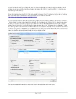
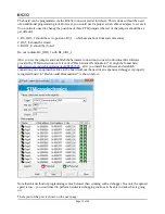
The port can be used for DFU USB mode of the STM32F107 processor. To be able to upload data you 
would need a mini USB cable connected to a personal computer that runs the proper software supplied by
ST.

Page 13 of 23

Summary of Contents for STM32-P107

Page 1: ...STM32 P107 development board User s manual All boards produced by Olimex are ROHS compliant Document revision L Feburary 2018 Copyright c 2014 OLIMEX Ltd All rights reserved Page 1 of 23 ...

Page 2: ...purpose are excluded This document is intended only to assist the reader in the use of the product OLIMEX Ltd shall not be liable for any loss or damage arising from the use of any information in this document or any error or omission in such information or any incorrect use of the product This evaluation board kit is intended for use for engineering development demonstration or evaluation purpose...

Page 3: ...VAC USB OTG connector capable of powering the board USB host connector 100 Mbit s Ethernet driver with RJ 45 connector RS232 driver with DE 09 female connector MiniSD card connector UEXT connector Two user programmable buttons Reset button and circuit Two user programmable LEDs Power on LED 25 Mhz quartz crystal Extension port connectors for many of microcontrollers pins Prototype area Easy to cha...

Page 4: ...rammers ARM JTAG ARM JTAG EW ARM USB OCD ARM USB OCD H ARM USB OCD TINY ARM USB OCD H Note that Olimex OpenOCD debuggers lack SWD interface by default There is the adapter ARM JTAG SWD that adds SWD to any of the programmers debuggers mentioned above Additionally you can use our ARM JTAG COOCOX debugger which has both JTAG and SWD interfaces and works with CooCox IDE natively and with IAR EW and K...

Page 5: ...rted peripherals timers ADCs DAC I2 Ss SPIs I2 Cs and USARTs Debug mode Serial wire debug SWD JTAG interfaces Cortex M3 Embedded Trace Macrocell 80 fast I O ports 80 I Os all mappable on 16 external interrupt vectors and almost all 5 V tolerant 10 timers four 16 bit timers each with up to 4 IC OC PWM or pulse counter and quadrature incremental encoder input 1 16 bit motor control PWM timer with de...

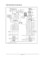
Page 6: ...STM32F107 BLOCK DIAGRAM Page 6 of 23 ...

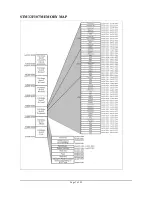
Page 7: ...STM32F107 MEMORY MAP Page 7 of 23 ...

Page 8: ...EN TIM2_CH4 48 PB12 SPI2_NSS I2S2_WS I2C2_SMBAL USART3_CK TIM1_BKIN CAN2_RX ETH_MII_TXD0 ETH_RMII_TXD0 51 PB13 SPI2_SCK I2S2_CK USART3_CTS TIM1_CH1N CAN2_TX ETH_MII_TXD1 ETH_RMII_TXD1 52 PB14 SPI2_MISO TIM1_CH2N USART3_RTS 53 PB15 SPI2_MOSI I2S2_SD TIM1_CH3N 54 PC0 ADC12_IN10 15 PC1 ADC12_IN11 ETH_MII_MDC ETH_RMII_MDC 16 PC2 ADC12_IN12 ETH_MII_TXD2 17 PC3 ADC12_IN13 ETH_MII_TX_CLK 18 PC4 ADC12_IN1...

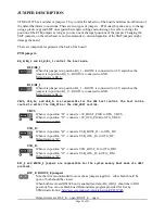
Page 9: ... compatible third party tool The programmed board power consumption is about 70 mA RESET CIRCUIT STM32 P107 reset circuit includes JTAG connector pin 15 U2 STE101P pin 28 RESET R73 10k R74 330Ohm R75 100Ohm 1 C55 100nF STM32F107 pin 14 NRST and RESET button CLOCK CIRCUIT Quartz crystal 25 MHz is connected to STM32F107 pin 12 OSC_IN and pin 13 OSC_OUT Quartz crystal 32 768kHz is connected to STM32F...

Page 10: ...per is in position B1_0 BOOT1 is connected to GND Default state is B1_0 VBUS USB_D and USB_D are responsible for the USB host control The host can be routed to either the USB_OTG or the USB_HOST control VBUS When is in position H connects 5V_HOST_PWR to OTG_VBUS When is in position O connects 5V_OTG_PWR to OTG_VBUS Default state is O USB_D When is in position H connects USB_HOST_D to OTG_DP When i...

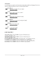
Page 11: ...3V analog power supply Default state is closed GNDA_E Enables board analog GND Default state is closed R T Connects RST to TRST Default state is open INPUT OUTPUT Status LED1 green with name STAT1 connected to STM32F107 pin 63 PC6 I2S2_MCK TIM3_CH1 Status LED2 yellow with name STAT2 connected to STM32F107 pin 64 PC7 I2S3_MCK TIM3_CH2 Power on LED red with name PWR this led shows that 3 3V is appli...

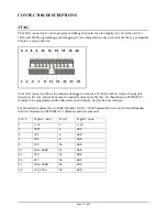
Page 12: ...p port directly to the core Instructions may be inserted and executed by the core thus allowing STM32F107 memory to be programmed with code and executed step by step by the host software For more details please refer to IEEE Standard 1149 1 1990 Standard Test Access Port and Boundary Scan Architecture and STM32F107 s datasheet and user s manual Pin Signal name Pin Signal name 1 3 3V 2 3 3V 3 TRST ...

Page 13: ...ed to provide 6 0V of voltage Pin Signal name 1 Power input 2 GND USB_HOST If you intend to use the USB_HOST connector pay attention to the position of VBUS USB_D and USB_D jumpers There is multiplexing between the USB_HOST connector and USB_OTG connector Pin Signal name 1 5V_HOST_PWR 2 USB_HOST_D 3 USB_HOST_D 4 GND USB_OTG If you intend to use the USB_OTG connector in host mode pay attention to t...

Page 14: ...cal user interface for DFU connection It is called DfuSe Demo Extract it and install the software Set the jumpers of STM32 P107 to boot from system memory Leave the rest of the jumpers as per default Connect the STM32 P107 board to the computer using a mini USB cable This would show an unrecognized device in Windows Device Manager Point the driver updater to the folder where DfuSe Demo was install...

Page 15: ... set the jumpers and establish the hardware connection you need to download the software provided by STMicroelectronics It is called Flash Loader Demonstrator It might be found here http www st com web en catalog tools PF257525 after you install the software and establish connection you can upload hex files to the board without the need of an expensive debugger A properly recognized board in Flash...

Page 16: ...ART I2C and SPI You can also find 3 3V power output and GND respectively pin 1 and pin 2 Pin Signal name 1 3 3V 2 GND 3 USART2_TX 4 USART2_RX 5 I2C1_SCL 6 I2C1_SDA 7 SPI3_MISO 8 SPI3_MOSI 9 SPI3_SCK 10 CS_UEXT SD MMC Pin Signal name 1 MCIDAT2 2 CS_MMC 3 SPI3_MOSI 4 3 3V 5 SPI3_SCK 6 GND 7 SPI3_MISO 8 MCIDAT1 9 Not connected 10 Not connected 11 Not connected 12 Not connected Page 16 of 23 ...

Page 17: ...hip side Pin Signal name chip side 1 TX 5 Not connected NC 2 TX 6 VDD 3 VDD 7 RX 4 Not connected NC 8 RX LED Color Usage Right Green Link status Left Yellow Activity status 3V_BAT Pin Signal name 1 VBAT 2 GND Page 17 of 23 ...

Page 18: ...MECHANICAL DIMENSIONS All measures are in mils Page 18 of 23 ...

Page 19: ... PE9 PE11 PE10 PE8 PE7 PE9 PE8 PE6 PE5 PE7 PE6 PE4 PE3 PE5 PE4 PE2 PE1 PE3 PE2 PC1 PC0 PE1 PE0 PC2 PC2 PC3 PC3 PC4 PC6 PC5 PC7 PC6 PC8 PC7 PC9 PC8 PC11 PC9 PC12 PC10 PC13 PC11 PC14 PB1 PB0 PB2 PB1 PB3 PB2 PB4 PB5 PB5 PB6 PB6 PB7 PB7 PB8 PB8 PB9 PB9 PB10 PB11 PB15 PB10 PB14 PD14 PD14 PD15 PD15 PD12 PD12 PD13 PD13 PD10 PD10 PD11 PD11 PD8 PD8 PD9 PD9 PD7 PD6 PD6 PD6 PD5 PD4 PD4 PD4 PD3 PD2 PD2 PD1 PD...

Page 20: ...oard s web page https www olimex com Products ARM ST STM32 P107 and wiki article https www olimex com wiki STM32 P107 Make sure that the demo you download is compatible with the board revision you have The board revision is printed on STM32 P107 itself Page 20 of 23 ...

Page 21: ...ated the information to fit board revision C updated schematics improved document layout added product support information updated links REV H improved information about bootloader REV I changed the schematic on page 8 REV J added picture of the protoarea pads with their respective labels REV K added new information about DFU mode hardware revision D changelog REV L February 2018 added table that ...

Page 22: ...the default EN level is opposite 7 All tantalum capacitors are changed to ceramic 8 Optimizations in the values of few other elements as well 9 R28 0R was changed to 10k C55 10uF 6 3V was added and RST connection was removed from the PHY rev D 1 All libraries were updated 2 SD MMC package was changed to TFC WPAPR 08 3 CD1 package was changed from 7 5mm to 5032 4 1nF 2kV X7R 1206 capacitor was adde...

Page 23: ...e allowed subject to a 10 restocking fee What is unaffected If you hooked it to power you affected it To be clear this includes items that have been soldered to or have had their firmware changed Because of the nature of the products we deal with prototyping electronic tools we cannot allow returns of items that have been programmed powered up or otherwise changed post shipment from our warehouse ...

Page 24: ...Mouser Electronics Authorized Distributor Click to View Pricing Inventory Delivery Lifecycle Information Olimex Ltd STM32 P107 ...

Reviews: