Special Registers
EBX-41 Reference Manual
66
Miscellaneous Control Register
This register is used to configure the control of the mSATA/PCIe Minicard slot multiplexer and
for controlling the SPI access.
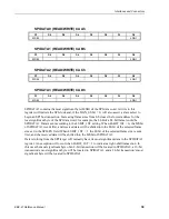
MISCCON (Read/Write) CAEh
D7
D6
D5
D4
D3
D2
D1
D0
Reserved
MUXSEL2
MUXSEL1
MUXSEL0
Reserved
Reserved
Reserved
ADIOMODE
Table 34: mSATA/PCIe Mux Control Register Bit Assignments
Bit
Mnemonic
Description
D7
Reserved
These bits are reserved. Only write 0 to these bits and ignore all read values.
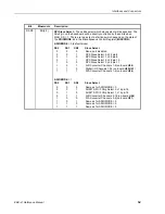
D6-D4
MUXSEL(2:0)
mSATA/PCIe Minicard Mux Controls (these are typically only configured in
the BIOS setup):
“000” Use only J8 Pin 43. This is based on a newer mSATA module
detection method recommended by Intel due to conflicts with J8 Pin 51.
Reliable for all PCIe Minicards but some mSATA modules do not ground this
so using setting “010” is recommended.
“001” Use only J8 Pin 51. This is only reliable for mSATA modules which
drive this signal High and is not recommended.
“010” Use either J8 Pin 43 or J8 Pin 51 to detect mSATA modules. This
works on the majority of modules and is the recommended setting. Note:
This is the BIOS default setting.
“011” Force the multiplexer to always be used as a PCIe Minicard.
“100” Force the multiplexer to always be used as an mSATA module.
“101” Undefined
“110” Undefined
“111” Undefined
D3-D1
Reserved
These bits are reserved. Only write 0 to this bit and ignore read values.
D0
ADIOMODE
Selects how the 3 bits in the SS field of the SPICONTROL register are
decoded (see decodings in the SPICONTROL register documentation):
0 Use standard decodes (primarily used if accessing more than 2 SPX
Expansion interface devices or on products with 8 analog inputs and 4
analog outputs or on products that do not use the SUMIT SPI interfaces).
This is the power-on-reset default setting.
1 Use alternate decodes (primarily used on products with 16 analog inputs
and 8 analog outputs or for accessing the SUMIT SPI interfaces).


