GV-395 Virtex-II DSP Hardware Accelerator Manual
GV & Associates, Inc.
07/10/04
7
4.0
Xilinx FPGA Configuration
The three Xilinx FPGAs may be configured three ways.
4.1
JTAG Cable Configuration
To use the JTAG download cable, the jumper block must be installed on JP1 and jumper block on JP9 must be
removed. The Virtex-II FGPA at U10 will be configured first, then the Virtex-II FPGA at U12, then the Virtex-II
FPGA at U14, then the Virtex-II FPGA at U16, and finally the Spartan II FPGA at U18. Attach the JTAP Cable to
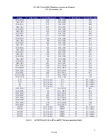
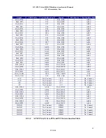
JP10 as follows: VCC ->1, GND->2, TDO -> 3, TDI -> 4, TCK ->5, TMS ->6. Pin 1 will be the pin closest to SW1.
4.2
Slave Serial Cable Configuration
To use the Slave Serial download cable, a jumper block must be installed on JP1 and JP9. The Virtex-II FGPA at
U10 will be configured first, then the Virtex-II FPGA at U12, then the Virtex-II FPGA at U14, then the Virtex-II
FPGA at U16, and finally the Spartan II FPGA at U18. Attach the Slave Serial Cable to JP5 as follows: VCC -> 1,
GND -> 2, CCLK -> 4, DONE -> 5, DIN -> 6, PROG -> 7, INIT -> 8, RST -> 9. Pin 1 will be the pin closest to
U13.
4.3
Parallel Down-Load Configuration
To use the parallel Flash EPROM (U2) to configure the Xilinx FPGAs, the jumper block at JP3 and JP9 must be
installed and the jumper block on JP2 must be removed. The EPROM file must be programmed from the
bottom up
.
This file must then be uploaded to the FLASH EPROM (U37) using the Slave Serial configuration mode. This is
further described in the section below. The Virtex-II FGPA at U10 will be configured first, then the Virtex-II FPGA
at U12, then the Virtex-II FPGA at U14, then the Virtex-II FPGA at U16, and finally the Spartan II FPGA at U18.
4.4
Slave Serial Programming of On-Board EEPROM (U2)
1.
Install the jumper blocks on JP1, JP2 and JP9.
2.
Remove the jumper blocks from JP3.
3.
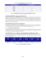
Using the Parallel Cable IV Programming Adapter, connect the Slave Serial cable to the JP5 of the GVA-
395 as shown in the table below.
4.
Apply power to the GVA-395.
5.
Press the reset button SW1.
6.
LED D41 will be lited for approximately 10 seconds while the Flash Memory is being erased.
7.
Wait for the LED D41 to extinguish.
8.
It is necessary to use the serial cable connection for the Programming Adapter in order to use a the slower
57 Kbps serial transfer rate.
9.
From the Xilinx Foundation Project Manager, select the Programming icon.
10.
Select the Hardware Debugger.
11.
From the Hardware Debugger, select the desire exo file to be programmed into the EEPROM. Please note
that the FPGA will also be programmed as the data is being written into the EEPROM.
12.
While the data is being written into the EEPROM, the LEDs D42 thru D44 will be toggling
13.
When all of the LED D41 thru D44 are lite, the program function has been completed.
14.
Remove power from the GVA-395 and remove the Slave Serial cable. Install that jumper blocks are install
on JP3 and JP9 with the jumper block on JP2 is removed. When power is reapplied, the GVA-395 will
configured from the EEPROM.


