3.5 Section 2: Timer Control
The timer-0 is used as the internal trigger A/D pacer timer. The timer-1 is designed for the
external trigger pacer timer. The timer-2 is used as the machine independent timer.
The timer-
2 is very important for settling time delay.
Refer to Intel
'
s
“
Microsystem Components
Handbook
"
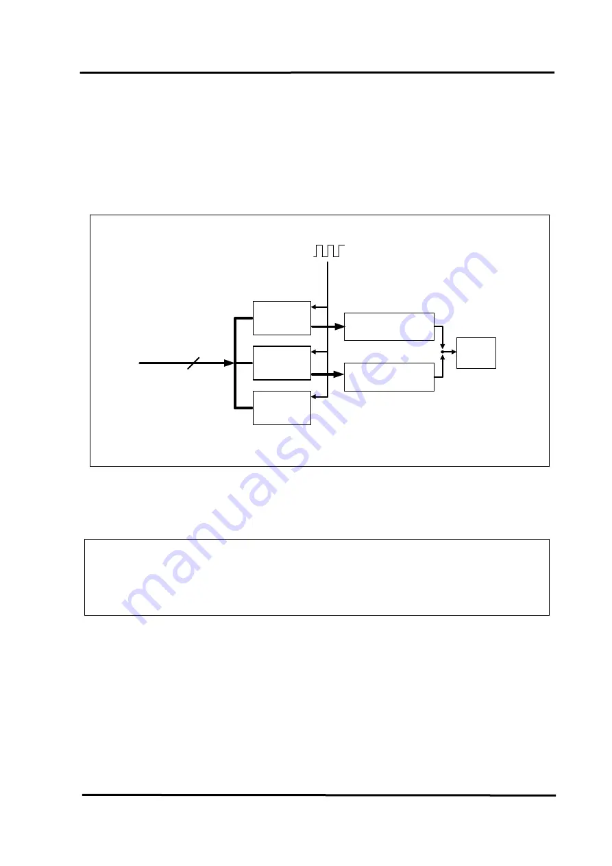
for 8254 programming. The block diagram of the 8254 timer is given as follows:
CLK
Timer 0
OUT0
CLK
Timer 1
OUT1
CLK
Timer 2
OUT2
8Mhz
Local Data Bus
Internal Pacer timer
External Pacer timer
ADC
Machine indenpedent Timer
D0,D1 ... D7
Figure 3-1: The block diagram of PCI-1202/1602/1800/1802 8254 timer.
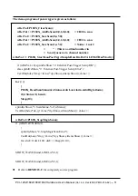
The I/O address of 8254 timer is given as follows:
z
I/O address of timer/counter_0 = wAd0*4
z
I/O address of timer/counter_1 = wAd1*4
z
I/O address of timer/counter_2 = wAd2*4
z
I/O address of control register = wAd3*4
PCI-1202/1602/1800/1802 Hardware User’s Manual
(
Ver.4.2, Dec/2009, PMH-014-42)---- 36


