BL652 Development Kit
User Guide
Embedded Wireless Solutions Support Center:
http://ews-support.lairdtech.com
www.lairdtech.com/bluetooth
7
© Copyright 2016 Laird. All Rights Reserved
Americas: +1-800-492-2320
Europe: +44-1628-858-940
Hong Kong: +852 2923 0610
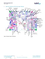
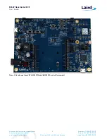
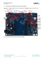
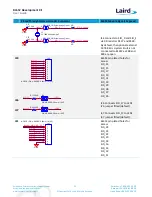
IO break-out 2.54 mm pitch pin header connectors (plated through-holes) that bring out all interfaces of
the BL652 module – UART, SPI, I2C, SIO [DIO or AIN (ADCs)], PWM, FREQ, NFC – and allow for plugging in
external modules/sensors.
Pin headers jumpers that allow the on-board sensors(I2C sensor, LEDs, Arduino SPI interface, etc.; and the
USB UART FTDI bridge) to be disconnected from BL652 module (by removing jumpers).
Three on-board sensors:
–
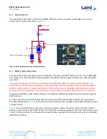
Analog output temperature sensor
–
I2C device (RTC chip)
–
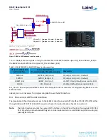
SPI device (EEPROM)
Two buttons and two LEDs for user interaction
NFC antenna connector on-board development board for use with supplied flexi-PCB NFC antenna
Optional external 32.768 kHz crystal oscillator. Not required for operation of the BL652; is disconnected by
open solder-bridges by default.
Optional external serial (SPI) flash IC. Not required for operation of the BL652; is disconnected by open
solder-bridges by default.
One analog buffer (provides a 3.3:1 attenuation) used when an analog source is at 5 volts into development
board.
Arduino connectors – Allow for plugging of Arduino shield boards.
Note:
The DVK-BL652 development board is not an Arduino shield, but is an Arduino base board (similar to
the Arduino UNO).
Arduino connector test points – All Arduino connector signals brought out to plated through-holes (2.54
mm pitch). Allow any Arduino connector signal (D0-D13 or A0-A5) to be connected to any BL652 module
using fly leads for maximum flexibility
Arduino connector signals wired to BL652 via headers or series resistors
Arduino connectors orientation at 90 degrees to the development board long dimension, allowing larger
Arduino shields to hang off the side of development board so not interfering with the mounted external
antenna or the BL652 module (the BLE chip antenna).
Access to BL652 JTAG – also known as Serial Wire Debug (SWD) Interface
On-board SWD (JTAG) programmer circuitry
smartBASIC runtime engine FW upgrade capability:
–
Via UART (using the FTDI USB-UART)
–
Via SWD (JTAG) using on-board JTAG programmer circuitry on the DVK-BL652
smartBASIC application upgrade capability:
–
Via UART (using the FTDI USB-UART)
–
Via OTA (Over-the-Air)


