BL652 Development Kit
User Guide
Embedded Wireless Solutions Support Center:
http://ews-support.lairdtech.com
www.lairdtech.com/bluetooth
15
© Copyright 2016 Laird. All Rights Reserved
Americas: +1-800-492-2320
Europe: +44-1628-858-940
Hong Kong: +852 2923 0610
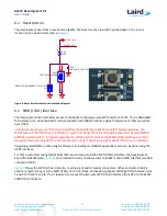
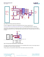
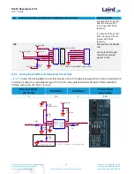
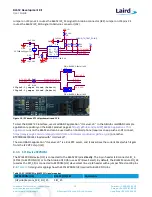
Figure 7: USB to SWD onboard circuitry routing
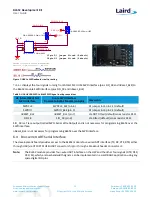
Table 2
displays the four signals running from Atmel MCU U14 SWD interface (plus SIO_18 and nReset_BLE) to
the BL652 module SWD interface (plus SIO_18 and nReset_BLE).
Table 2: USB U4 USB-SWD to BL652 SWD signal routing connections
U4 (Atmel MCU) Net
SWD Interface
Route SWD Interface
from U4 to BL652 Module (and pin)
Comments
SWDCLK
SWDCLK_BLE (pin 6)
Fit jumper in J4 pin 2-1 (default)
SWDIO
SWDIO_BLE (pin 5)
Fit jumper in J3 pin 2-1 (default)
nRESET_BLE
nRESET_BLE (pin 7)
Via NOT Fitted (default)series resistor R111
SIO.18
SIO_18 (pin 9)
Via Fitted (default) series resistor R121
SIO_18 is a Trace output (called SWO, Serial Wire Output) and is not necessary for programming BL652 over the
SWD interface.
nReset_BLE is not necessary for programming BL652 over the SWD interface.
6.4
Four-wire UART Serial Interface
The development board provides access to the BL652 module four-wire UART interface (TX, RX, CTS, RTS) either
through USB (via UT10 FTDI USB-UART convertor chip) or through a breakout header connector J1.
Note:
The BL652 module provides four-wire UART interface on the HW and the other four signals (DTR, DSR,
DCD, RI), which are low bandwidth signals, can be implemented in a smartBASIC application using any
spare digital SIO pins.
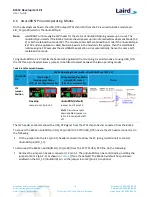
SEGGER J-Link Lite Cortex M-9 JTAG/SWD
Emulator 10-pin connector. Top view.
GND
SWDIO
VCC_IO
SWDCLK
JP1
PIN HEADER,1.27mm 2X5P
1
2
3
4
5
6
7
8
9
10
PIN HEADER,2.54mm 1X3P
J3
1
1
2
2
3
3
J3pin2-1 jumper fitted (Default).
J4pin2-1 jumper fitted (Default).
PIN HEADER,2.54mm 1X3P
J4
1
1
2
2
3
3
SWDCLK_BLE
nRESET_BLE
SIO_18
SWDIO_BLE

