CDV Construction Manual – Issue 3
Page 7
3
C
IRCUIT
D
ESCRIPTION
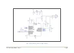
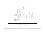
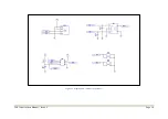
Integrated circuit U2 is a Si5351A clock generator chip. A 25MHz crystal supplies the master
clock on pins 2 and 3. The Si5351A is controlled over a shared I2C bus by microcontroller U1.
The 3.3V power supply rail is applied to pins 1 and 7. Capacitors C8 andC12 and a ferrite bead
help guard against instability and decouple the IC from the power supply. The variable output
(VFO) appears on pin 10 and is capacitively coupled by C5 to the VFO output connector.
Similarly the fixed frequency output on pin 9 is capacitively coupled by C11 to the FIX output
connector.
The output signals from the Si5351A are square wave in shape with a frequency spectrum being
almost entirely comprised of odd harmonics. While this is adequate for most situations, an
external add-on attenuator filter board is available for more demanding applications. See
section 11 for more details.
The microcontroller is an Atmel ATmega328 and runs an internal 8MHz clock which avoids the
need for an external crystal. It controls the OLED and Si5351A over a common I2C bus on pins
28 and 27. The I2C standard calls for bus pull-up resistors and this is achieved through two 4.7K
resistors R7 and R8.
A rotary encoder produces quadrature signals when rotated and one line (REA) is fed into the
microcontroller interrupt input (pin 32) and becomes the reference input. Once an interrupt is
detected the state of the other line (REB) is read and the direction determined. The rotary
encoder also incorporates a press button switch input on U1 pin 1 and is used for a number of
functions as described later. U1 incorporates pull-up resistors for the encoder inputs so they are
normally held high and capacitors C9 and C10 help limit encoder switch bounce.
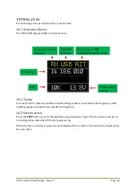
The CDV uses a small 0.96 inch monochrome 128 x 64 pixel matrix OLED for display. If
characters were written unmodified to the matrix they would be small and difficult to read, so
the firmware combines pixels to write larger characters with 4 rows of 10 characters. The OLED
does not require a backlight and has excellent brightness and contrast in high ambient light
levels. It is also controlled through the common I2C bus.
The microcontroller has an internal analog to digital converter (ADC) which measures the
incoming power supply rail via a resistive attenuator formed with R3 and R4. The calculated
value is displayed on the OLED during use.
The microcontroller monitors the state of the TX/RX input on pin 31, while the state of the
USB/LSB input is monitored on pin 30. The inputs are attenuated by 22K resistors and the
microcontroller inputs are further protected by 3.3V Zener diodes. The inputs are considered
low when the input is below about 3.3V. An input above 3.3V is considered a high. The inputs
can handle up to 20V levels.
The incoming power supply is regulated to 3.3V by a 78L33 100mA regulator which has its tab
soldered to the PCB groundplane to act as a heatsink. The 3.3V rail powers the microcontroller,
Si5351A and the OLED. Diode D1 provides reverse polarity protection. When the power supply
is connected in reverse, the diode will not conduct and the main circuits will be protected.
The PCB also includes space to fit an ISP connector to allow future software upgrades.
Summary of Contents for CDV
Page 1: ...CDV Construction Manual Issue 3 Page 1 CDV COMPACT DIGITAL VFO CONSTRUCTION MANUAL ...
Page 8: ...CDV Construction Manual Issue 3 Page 8 Figure 1 Microcontroller and power supply schematic ...
Page 9: ...CDV Construction Manual Issue 3 Page 9 Figure 2 Si5351A Clock generator schematic ...
Page 10: ...CDV Construction Manual Issue 3 Page 10 Figure 3 Display and controls schematic ...
Page 30: ...CDV Construction Manual Issue 3 Page 30 Figure 11 Attenuator filter board fitted to the CDV ...


