Hardware Description
5
4. Hardware Description
4.1. Mechanics
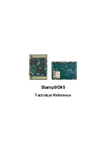
The Stamp9G45 was designed as a flexible CPU-Module, which can be connected to base
boards via 2x 100-pin fine pitch low profile Hirose
®
FX8 connectors
The size of the Stamp9G45's PCB is only 53.6x38x6.0 mm fitting it in even the smallest
design. While having implemented the sensible CPU, DDRAM and Flash design it still
exports almost all possible CPU-Pins on it's connectors to allow a flexible design on base
boards
The Stamp9G45 has an on-board Micro SD-Card slot, thus supporting even large memories
needs in its compact design
4.2. AT91SAM9G45 Processor Core
The AT91SAM9G45 runs at 400 MHz with a memory bus frequency of 132 MHz.
Here are some of the most important features of the SAM9G45 ARM926EJ-S core:
• 32 Kbyte Data Cache, 32 Kbyte Instruction Cache, Write Buffer
• Two 32 Bit Data Bus
• ARM v4 and v5 Memory Management Unit (MMU)
• ARM v5 32-bit Instruction Set, ARM Thumb 16-bit Instruction Set supported
• DSP Instruction Extensions
• ARM Jazelle
®
Technology for Java
®
Acceleration
• EmbeddedICE
™
Debug Communication Channel Support
Some of these features - like Jazelle - are currently not supported by the operating system
of the product.
4.3. Memory
The Stamp9G45 is equipped with two 32-Bit external bus interfaces, EBI0 and EBI1. Only a
16-Bit bus of EBI0 is exported on the interface connectors of the Stamp9G45. The memory
bus voltage is 1.8 V and runs at 133 MHz. The memory bus voltage is different from normal
operating voltage, which is 3.3 V. This has to be considered, when designing additional
peripherals connected to the memory bus. Eventually buffer chips are necessary.
4.3.1. NAND Flash
The Stamp9G45 is equipped with a 128 MB NAND flash with 100000 erase and write
cycles.It is organized in 128KB blocks. Customer specific adaptations are possible up
to 1 GB on-board NAND flash. It is connected to chip select three (NCS3) of the
microcontroller.

