SARA-G3 series - System Integration Manual
UBX-13000995 - R06
Objective Specification
Design-in
Page 136 of 218
2.5.3
DDC (I
2
C) interface
2.5.3.1
Guidelines for DDC (I
2
C) circuit design
The
SDA
and
SCL
lines must be connected to the DDC (I
2
C) interface pins of the u-blox GNSS
receiver (i.e. the SDA2 and SCL2 pins of the u-blox positioning receiver) on the application board to
allow the communication between the wireless module and the u-blox GNSS receiver, enabled by the
AT+UGPS command (for more details refer to
u-blox AT Commands Manual [2]).
To be compliant to the I
2
C bus specifications, the module bus interface pads are open drain output and
pull up resistors must be used conforming to the
I
2
C bus specifications [13]. Since the pull-up resistors
are not mounted on the module, they must be mounted externally.
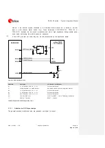
Provide external pull-ups resistors (e.g. 4.7 k
) on
SDA
and
SCL
lines and connect them to the
V_INT
1.8 V supply source, or another 1.8 V supply source enabled after
V_INT
(e.g., as the 1.8
V supply present in the application circuit of
, controlled by the wireless
module).
The signal shape is defined by the values of the pull-up resistors and the bus capacitance. Long wires
on the bus increase the capacitance. If the bus capacitance is increased, use pull-up resistors with
nominal resistance value lower than 4.7 k
, to match the
I
2
C bus specifications [13] regarding rise and
fall times of the signals.
Capacitance and series resistance must be limited on the bus to match the I
2
C specifications (1.0
µs is the maximum allowed rise time on the
SCL
and
SDA
lines): route connections as short as
possible.
If the pins are not used as DDC bus interface, they can be left unconnected.
The following special features over GPIOs can be optionally implemented on the application board to
improve the integration of SARA-G350 wireless modules with a u blox GNSS receiver:
The
GPIO2
, by default configured to provide the “GNSS supply enable” function, must be connected
to the active-high enable pin (or the active-low shutdown pin) of the voltage regulator that supplies
the u-blox positioning receiver on the application board to enable or disable the supply of the u-blox
GNSS receiver connected to the wireless module by the AT+UGPS command
The
GPIO3
, by default configured to provide the “GNSS data ready” function, must be connected to
the data ready output of the u-blox positioning receiver (i.e. the pin TXD1 of the u-blox GNSS
receiver) on the application board, to sense when the u-blox positioning receiver connected to the
wireless module is ready to send data by the DDC (I
2
C) interface
The
GPIO4
, by default configured to provide the “GNSS RTC sharing” function, must be connected to
the RTC synchronization signal of the u-blox positioning receiver (i.e. the pin EXTINT0 of the u-blox
GNSS receiver) on the application board, to provide an RTC (Real Time Clock) synchronization
signal at the power up of the u-blox positioning receiver connected to the wireless module


