background image


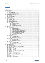
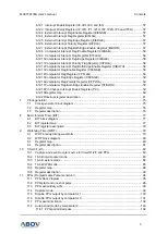
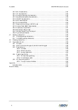
MC97F6108A 

User’s Manual


16 MHz 8-bit Microcontroller 


8KB Flash, 12-bit ADC, Analog Comparator and OP-AMP


User’s Manual Version 1.12 


Global Top Smart MCU Innovator 

www.abovsemi.com


Introduction 

This 

user’s

 manual targets application developers who use MC97F6108A for their specific needs. This 

document provides complete information of how to use MC97F6108A device. Standard functions and 
blocks including corresponding register information of MC97F6108A are introduced in each chapter, 
while instruction set is in Appendix. 

MC97F6108A is based on M8051 core, and provides standard features of 8051 such as 8-bit ALU, PC, 
8-bit registers, timers and counters, serial data communication, PSW, DPTR, SP, 8-bit data bus and 
2x16-bit address bus, and 8/11/16-bit operations. 

In addition, this device offers highly flexible and cost effective solutions with the following peripherals 
inside: 8Kbytes of FLASH, 256bytes of IRAM, 256bytes of XRAM, General Purpose I/Os, Basic Interval 
Timer, Watchdog Timer, 16-bit timer/counter, 16-bit PWM output, 16-bit PPG output, UART, I2C, 12-bit 
A/D Converter, analog comparator, on-chip OP-AMP, buzzer driving port, on-chip POR, LVR, BOD, on-
chip oscillator and clock circuitry. 

As a field proven best seller, MC97F6108A has been sold more than 3 billion units up to now, and 
introduces rich features such as excellent noise immunity, code optimization, cost effectiveness, and 
so on. 

Reference document 


MC97F6108A  programming  tools  and  manuals  released  by  ABOV:  They  are  available  at 
ABOV website, 

www.abovsemi.com

. 


SDK-

51  User’s  guide

  (System  Design  Kit)  released  by  Intel  in  1982:  It  contains  all  of 

components of a single-

board computer based on Intel’s 8051 single

-chip microcomputer. 


Information on Mentor Graphics 8051 microcontroller: The technical document is provided at 
Mentor

 website: 

https://www.mentor.com/products/ip/peripheral/microcontroller/


Summary of Contents for MC97F6108A

Page 1: ...solutions with the following peripherals inside 8Kbytes of FLASH 256bytes of IRAM 256bytes of XRAM General Purpose I Os Basic Interval Timer Watchdog Timer 16 bit timer counter 16 bit PWM output 16 b...

Page 2: ...egister PxOD 36 5 1 5 De bounce Enable Register PxDB 36 5 1 6 Port Selection Register psrx 36 5 1 7 Register map 37 5 2 P0 port 38 5 2 1 P0 port description 38 5 2 2 Register description for P0 38 5 3...

Page 3: ...ity Register CFPOLA 59 6 12 17Comparator Flag Both Edge Enable Register CFBOTH 59 6 12 18Pin Change Interrupt Enable Register PCI 59 6 12 19Register map 60 6 12 20Interrupt register description 61 7 C...

Page 4: ...ation 142 14 4 Register map 143 14 5 Register description 144 15 USART 147 15 1 Block diagram 148 15 2 Clock generation 149 15 3 External clock XCK 150 15 4 Synchronous mode operation 150 15 5 Data fo...

Page 5: ...on 197 19 Memory programming 199 19 1 Flash control and status registers 199 19 1 1 Register map 199 19 1 2 Register description 200 19 2 Memory map 206 19 2 1 Flash memory map 206 19 3 Serial in syst...

Page 6: ...age range 232 20 21 Recommended circuit and layout 232 20 22 Typical characteristics 233 21 Package information 235 21 1 20 SOP package information 235 21 2 16 SOPN package information 236 22 Ordering...

Page 7: ...errupt Return Instruction 56 Figure 23 Clock Generator Block Diagram 75 Figure 24 Basic Interval Timer Block Diagram 77 Figure 25 Watchdog Timer Interrupt Timing Waveform 79 Figure 26 Watchdog Timer B...

Page 8: ...Bit 156 Figure 72 Stop Bit Sampling and Next Start Bit Sampling 156 Figure 73 SPI Clock Formats when UCPHA 0 158 Figure 74 SPI Clock Formats when UCPHA 1 159 Figure 75 I2C Block Diagram 168 Figure 76...

Page 9: ...rupt 230 Figure 114 STOP Mode Release Timing when Initiated by RESETB 230 Figure 115 Operating Voltage Range 232 Figure 116 Recommended Voltage Range 232 Figure 117 Output High Voltage VOH 233 Figure...

Page 10: ...tor Frequencies 166 Table 24 Register Map 179 Table 25 Peripheral Operation Status during Power Down Mode 184 Table 26 Power Down Operation Register Map 189 Table 27 Hardware Setting Values in Reset S...

Page 11: ...Internal Flash ROM Characteristics 231 Table 56 Input Output Capacitance 231 Table 57 MC97F6108A Device Ordering Information 237 Table 58 Pins for Flash Programming 241 Table 59 OCD II Features 243 Ta...

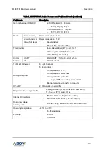
Page 12: ...unts Peripherals Description Core CPU 8 bit CISC core M8051 2 clocks per cycle Interrupt Up to 23 peripheral interrupts supported EINT0 EINT1 EINT2 PCI 4 Comparator output 5 I2C 1 USART 2 Timer 0 1 2...

Page 13: ...it x 4 ch T0 T1 T2 T3 Comm function USART 8 bit USART x 1 ch or 8 bit SPI x 1 ch I2C 8 bit I2C x 1 ch 12 bit A D Converter 8 input channels Analog comparator 5 Comparators 1 Comparator for Sync 1 Comp...

Page 14: ...or Clock generator 16MHz Internal RC OSC 8kHz Internal WDT OSC Voltage Down convertor CORE M8051 General purpose I O 18 ports normal I O with analog input Watchdog timer 1 channel 8 bit 8kHz internal...

Page 15: ...1I P20 AN5 AMP2O P17 AN7 AVREF AMP1O P16 CMP0_IN_N P15 CMP0_IN_P P14 CMP2_IN_P P13 CMP1_IN_P P12 DSDA1 P11 DSCL1 NOTES 1 Monitor function P01 CMPXO P07 TPPGO 2 USART function P01 XCK P04 TXD P03 RXD 3...

Page 16: ..._P P14 CMP2_IN_P P13 CMP1_IN_P NOTES 1 Monitor function P01 CMPXO P07 TPPGO 2 USART function P01 XCK P04 TXD P03 RXD 3 SPI function P02 SS P04 MOSI P03 MISO P01 SCK when USART is used as SPI mode 4 I2...

Page 17: ...CL IOU OCD debugger clock Pull up 5 4 P03 IOUS Port 0 bit 3 Input output RXD I USART data receive SDA IO I2C data signal EINT1 I External interrupt input ch 1 AN2 IA ADC input ch 2 6 5 P04 IOUS Port 0...

Page 18: ...oltage AMP1O O OP AMP 1 output 18 14 P20 IOUS Port 2 bit 0 Input output AN5 IA ADC input ch 5 AMP2O O OP AMP 2 output 19 15 P21 IOUS Port 2 bit 1 Input output AMP1I I OP AMP 1 input 1 1 VDD P VDD 20 1...

Page 19: ...figures 1 2 and 3 regarding general purpose I O port and external interrupt I O port respectively DATA REGISTER DIRECTION REGISTER PORTx INPUT PAD VDD VDD Schmitt Level Input Level Shift 1 8V to ExtV...

Page 20: ...NPUT PAD VDD VDD MUX MUX 0 1 MUX 1 0 0 1 Schmitt Level Input VDD Level Shift 1 8V to ExtVDD Level Shift ExtVDD to 1 8V OPEN DRAIN REGISTER PULL UP REGISTER VDD If one sub function is selected the dire...

Page 21: ...IRECTION REGISTER PORTx INPUT PAD VDD VDD Schmitt Level Input Level Shift 1 8V to ExtVDD Level Shift ExtVDD to 1 8V MUX 1 0 Analog Channel enable ANALOG INPUT Digital Input blocking enable OPEN DRAIN...

Page 22: ...his logical separation of the memory 8 bit CPU address can access the Data Memory more rapidly 16 bit Data Memory address is generated through the DPTR register MC97F6108A provides on chip 8Kbytes of...

Page 23: ...1 for example is assigned to location 000BH If the external interrupt 11 is going to be used its service routine must begin at location 000BH If the interrupt is not going to be used its service locat...

Page 24: ...d into 4 banks of 8 registers Program instructions call out these registers as R0 through R7 Two bits in the Program Status Word select which register bank is in use This allows more efficient use of...

Page 25: ...5E 5D 5C 5B 5A 59 58 57 56 55 54 53 52 51 50 4F 4E 4D 4C 4B 4A 49 48 47 46 45 44 43 42 41 40 3F 3E 3D 3C 3B 3A 39 38 37 36 35 34 33 32 31 30 2F 2E 2D 2C 2B 2A 29 28 27 26 25 24 23 22 21 20 1F 1E 1D 1...

Page 26: ...s of XRAM and 256bytes of XSFR This area has no relation with RAM FLASH It can be read and written to through SFR with 8 bit unit External RAM 256bytes Indirect Addressing 0000H 00FFH 2FFFH 2F00H Exte...

Page 27: ...I2CSAR1 I2CSAR 0C8H CFFLAG DSTEP T3CR T3CR1 PWM3DRL CDR3L T3L PWM3DRH CDR3H T3H PWM3PRL T3DRL PWM3PRH T3DRH 0C0H CFEDGE USTEP T2CR T2CR1 PWM2DRL CDR2L T2L PWM2DRH CDR2H T2H PWM2PRL T2DRL PWM2PRH T2DRH...

Page 28: ...0EH 07H 0FH 2F78H 2F70H 2F68H 2F60H 2F58H 2F50H 2F48H PSR0 PSR2 PSR3 2F40H 2F38H CA_REGA CA_REGB CA_REGC 2F30H CA_REG0 CA_REG1 CA_REG2 CA_REG3 CA_REG4 CA_REG5 CA_REG6 CA_REG7 2F28H 2F20H 2F18H 2F10H P...

Page 29: ...ata Register P2 R W 0 0 91H P1 Direction Register P1IO R W 0 0 0 0 0 0 0 0 92H Interrupt Priority Register IP R W 0 0 0 0 0 0 93H Interrupt Priority Register High IPH R W 0 0 0 0 0 0 94H Pin Change In...

Page 30: ...0DRL W 0 0 0 0 0 0 0 0 B5H Timer 0 Register High T0H R 0 0 0 0 0 0 0 0 Capture 0 Data Register High CDR0H R 0 0 0 0 0 0 0 0 PWM 0 Duty Register High PWM0DRH W 0 0 0 0 0 0 0 0 B6H Timer 0 Data Register...

Page 31: ...R 0 0 0 0 0 0 0 0 PWM 3 Duty Register High PWM3DRH W 0 0 0 0 0 0 0 0 CEH Timer 3 Data Register Low T3DRL W 1 1 1 1 1 1 1 1 PWM 3 Period Register Low PWM3PRL W 1 1 1 1 1 1 1 1 CFH Timer 3 Data Register...

Page 32: ...W 0 0 0 0 0 0 0 0 EEH BUZZER Control Register BUZCR R W 0 0 0 0 0 EFH BUZZER Data Register BUZDR R W 1 1 1 1 1 1 1 1 F0H B Register B R W 0 0 0 0 0 0 0 0 F1H Auto Period Mode Period High Register ATP...

Page 33: ...R W 0 0 0 0 0 0 0 0 2F0EH PPG Off Time Min Period Low Register OFFMINLR R W 0 0 0 0 0 0 0 0 2F0FH PPG Off Time Min Period High Register OFFMINHR R W 0 0 0 0 0 0 0 0 2F10H P2 Pull up Resistor Selectio...

Page 34: ...SP Stack Pointer 81H 7 6 5 4 3 2 1 0 SP R W R W R W R W R W R W R W R W Initial value 07H SP Stack Pointer DPL Data Pointer Register Low 82H 7 6 5 4 3 2 1 0 DPL R W R W R W R W R W R W R W R W Initia...

Page 35: ...y Flag F0 General Purpose User Definable Flag RS1 Register Bank Select bit 1 RS0 Register Bank Select bit 0 OV Overflow Flag F1 User Definable Flag P Parity Flag Set Cleared by hardware each instructi...

Page 36: ...n be connected to I O ports individually with a pull up resistor selection register PxPU The pull up register selection controls the pull up resister enable disable of each port When the corresponding...

Page 37: ...P1IO 91H R W 00H P1 Direction Register P1PU 2F08H R W 00H P1 Pull up Resistor Selection Register P1OD 2F09H R W 00H P1 Open drain Selection Register P1DB 2F0AH R W 00H P1 De bounce Enable Register P2...

Page 38: ...R W R W Initial value 00H P0 7 0 I O Data P0IO P0 Direction Register 89H 7 6 5 4 3 2 1 0 P07IO P06IO P05IO P04IO P03IO P02IO P01IO P00IO R W R W R W R W R W R W R W R W Initial value 00H P0IO 7 0 P0...

Page 39: ...the sampling clock the signal is eliminated as noise 2 A pulse level should be input for the duration of 3 clock or more to be actually detected as a valid edge 3 The port de bounce is automatically d...

Page 40: ...t or AMP2O output PSR24 P0 6 Analog Input selection register 0 P0 6 digital input default 1 P0 6 AIN 4 input PSR23 P0 4 Analog Input selection register 0 P0 4 digital input default 1 P0 4 AIN 3 input...

Page 41: ...t 1 P1 6 CMP0_IN_N input PSR33 P1 5 Analog Input selection register 0 P1 5 digital input default 1 P1 5 CMP0_IN_P input PSR32 P1 4 Analog Input selection register 0 P1 4 digital input default 1 P1 4 C...

Page 42: ...R W R W Initial value 00H P1 7 0 I O Data P1IO P1 Direction Register 91H 7 6 5 4 3 2 1 0 P17IO P16IO P15IO P14IO P13IO P12IO P11IO P10IO R W R W R W R W R W R W R W R W Initial value 00H P1IO 7 0 P1...

Page 43: ...isable 1 Enable NOTES 1 If the same level is not detected on enabled pin three or four times in a row at the sampling clock the signal is eliminated as noise 2 A pulse level should be input for the du...

Page 44: ...P2 P2 P2 Data Register 90H 7 6 5 4 3 2 1 0 P21 P20 R W R W Initial value 00H P2 1 0 I O Data P2IO P2 Direction Register 99H 7 6 5 4 3 2 1 0 P21IO P20IO R W R W Initial value 00H P2IO 1 0 P2 Data I O D...

Page 45: ...MC97F6108A User s manual 5 I O ports 45 P2DB P2 De bounce Enable Register 2F02H 7 6 5 4 3 2 1 0 P21DB P20DB R W R W Initial value 00H P2DB 1 0 Configure de bounce of P2 port 0 Disable 1 Enable...

Page 46: ...imultaneously Each interrupt source can be controlled by EA bit and each IEx bit Interrupt latency of 5 to 8 machine cycles in single interrupt system A non maskable interrupt is always enabled while...

Page 47: ...ity levels are received simultaneously the request of higher priority level is served prior to the lower one level 0 INT0 INT1 INT2 INT3 INT5 INT6 INT7 INT8 INT9 INT11 INT12 INT13 INT14 INT15 level 1...

Page 48: ...external interrupt source has enable disable bits External interrupt flag register EIFLAG indicates the status of external interrupts EIBOTH EIEDGE EIPOLA EINT0 Pin EINT1 Pin EIFLAG0 EIFLAG1 EINT0 In...

Page 49: ...rrupt flags Comparator0 debounce output Comparator1 debounce output Comparator2 debounce output Comparator3 debounce output CMP0IF CMP1IF CMP2IF CMP3IF CMP0 Interrupt CMP1 Interrupt CMP2 Interrupt CMP...

Page 50: ...CH CMP1IF CMP2IF CMP3IF CMP4IF CMP1 CMP2 CMP3 CMP4 CIFLAG 1 ACH CIFLAG 2 ACH CIFLAG 3 ACH CIFLAG 4 ACH IIF I2C I2CMR 7 DAH RXC USTAT 5 FDH RXD TXC TXD USTAT 6 FDH TMIF0 T0 TMISR 0 D5H TMIF1 T1 TMISR 1...

Page 51: ...e 003BH CMP2 Interrupt INT8 IE1 2 9 Maskable 0043H CMP3 Interrupt INT9 IE1 3 10 Maskable 004BH CMP4 Interrupt INT10 IE1 4 11 Maskable 0053H I2C Interrupt INT11 IE1 5 12 Maskable 005BH RXD Interrupt IN...

Page 52: ...rent instruction it needs 3 to 9 machine cycles to go to the interrupt service routine The interrupt service task is terminated by the interrupt return instruction RETI Once an interrupt request is ge...

Page 53: ...ming of Interrupt Enable Register Case B in Figure 17 shows the effective time after controlling Interrupt Flag Registers Figure 17 Effective Timing of Interrupt Flag Register Interrupt Enable Registe...

Page 54: ...routine is executed If the priority level of INT0 is same or lower than INT1 INT0 will be served after the INT1 service has completed An interrupt service routine may be only interrupted by an interr...

Page 55: ...ddress and the Entry Address of ISR 6 10 Saving restore general purpose registers Figure 21 Saving Restore Process Diagram and Sample Source Interrupt latched Interrupt goes active System Clock Max 4...

Page 56: ...nterrupt Return Instruction Interrupt sources are sampled at the last cycle of a command If an interrupt source is detected the lower 8 bit of interrupt vector INT_VEC is decided M8051EW core makes in...

Page 57: ...n be cleared to disable external interrupt by writing 0 on to themselves 6 12 4 External Interrupt Flag Register EIFLAG External Interrupt Flag Register EIFLAG is set to 1 when the pin changeable inte...

Page 58: ...nterrupt Polarity Flag Register CIPOLA determines a level type from high and low level or determined an edge type from rising and falling edge of comparator comparator0 to comparator 4 interrupt Initi...

Page 59: ...sing and falling edge of comparator comparator0 to comparator 4 flag Initially default value is to occur interrupt at high level or rising edge 6 12 17 Comparator Flag Both Edge Enable Register CFBOTH...

Page 60: ...R W 00H External Interrupt Flag Enable Register EIFLAG A4H R W 00H External Interrupt Flag Register EIEDGE A5H R W 00H External Interrupt Flag Edge Register EIPOLA A6H R W 00H External Interrupt Flag...

Page 61: ...rrupt bits 0 All Interrupt disable 1 All Interrupt enable INT5E Enable or Disable ATP_MAX Interrupt 0 Disable 1 Enable INT4E Enable or Disable ATP_MIN Interrupt 0 Disable 1 Enable INT3E Enable or Disa...

Page 62: ...INT11E Enable or Disable I2C Interrupt 0 Disable 1 Enable INT10E Enable or Disable Comparator4 Interrupt 0 Disable 1 Enable INT9E Enable or Disable Comparator3 Interrupt 0 Disable 1 Enable INT8E Enabl...

Page 63: ...ue 00H INT17E Enable or Disable Timer 3 Interrupt 0 Disable 1 Enable INT16E Enable or Disable Timer 2 Interrupt 0 Disable 1 Enable INT15E Enable or Disable Timer 1 Interrupt 0 Disable 1 Enable INT14E...

Page 64: ...DT Interrupt 0 Disable 1 Enable INT19E Enable or Disable ADC Interrupt 0 Disable 1 Enable INT18E Enable or Disable PPG Interrupt 0 Disable 1 Enable IP Interrupt Priority Register 92H 7 6 5 4 3 2 1 0 I...

Page 65: ...0 level 0 lowest 0 1 level 1 1 0 level 2 1 1 level 3 highest IP2 Interrupt Priority Register 2 9CH 7 6 5 4 3 2 1 0 IP25 IP24 IP23 IP22 IP21 IP20 R W R W R W R W R W R W Initial value 00H IP2H Interru...

Page 66: ...el 0 lowest 0 1 level 1 1 0 level 2 1 1 level 3 highest EIENAB External Interrupt Flag Enable Register A3H 7 6 5 4 3 2 1 0 ENAB2 ENAB1 ENAB0 R W R W R W Initial value 0H ENAB2 Enable or Disable Extern...

Page 67: ...ernal Interrupt 2 occurs this bit is set 0 External Interrupt2 not occurred 1 External Interrupt2 occurred FLAG1 When External Interrupt 1 occurs this bit is set 0 External Interrupt1 not occurred 1 E...

Page 68: ...hen Low level or falling edge Interrupt occurs POLA0 Determine the polarity of External Interrupt 0 0 When High level or rising edge Interrupt occurs default 1 When Low level or falling edge Interrupt...

Page 69: ...nterrupt CIFLAG Comparator Interrupt Flag Register ACH 7 6 5 4 3 2 1 0 CMP4IF CMP3IF CMP2IF CMP1IF CMP0IF R W R W R W R W R W Initial value 00H When an interrupt source is generated and CIENAB is set...

Page 70: ...nitial value 00H According to CIEDGE this register acts differently If CIEDGE is level type comparator interrupt polarity have level value If CIEDGE is edge type comparator interrupt polarity have edg...

Page 71: ...on Disable default 1 Both edge detection Enable CIBOTH0 Determine the type of Comparator0 Interrupt 0 Both edge detection Disable default 1 Both edge detection Enable CFENAB Comparator Flag Enable Reg...

Page 72: ...rator2 occurred C1_FLAG When Comparator1 occurs this bit is set 0 Comparator1 not occurred 1 Comparator1 occurred C0_FLAG When Comparator0 occurs this bit is set It is cleared automatically when PPG p...

Page 73: ...ising edge flag occurs default 1 When Low level or falling edge flag occurs CFPOLA0 Determine the polarity of Comparator0 flag 0 When High level or rising edge flag occurs default 1 When Low level or...

Page 74: ...sable of P1 6 0 Disable default 1 Enable PCI 5 Select PCI interrupt enable or disable of P1 5 0 Disable default 1 Enable PCI 4 Select PCI interrupt enable or disable of P1 4 0 Disable default 1 Enable...

Page 75: ...and ports de bounce on POR is recommended Oscillators in the clock generator are introduced in the followings Calibrated high internal RC oscillator 16MHz INTRC OSC 1 16MHz default system clock INTRC...

Page 76: ...lect WDTRC oscillator on or off 0 WDTRC off default 1 WDTRC on CHBS Control the scheme of clock change If this bit set to 0 clock change is controlled by hardware But if this set to 1 clock change is...

Page 77: ...r interrupt 8 1 BIT block diagram In this section basic interval timer of MC97F6108A is described in a block diagram BITR 8 bit COUNT BIT_CLK BIT Interrupt Generator BIT Out Generator BIT Interrupt Fl...

Page 78: ...IT 256 1 0 fBIT 16 1 1 fBIT 2 BWDTRC Select BIT Clock Source fBIT to WDTRC 0 fSYS 1 fWDTRC BCLR If this bit is written to 1 BIT Counter is cleared to 0 After one machine cycle BCLR is cleared automati...

Page 79: ...unts up After 1 machine cycle this bit is cleared to 0 automatically The WDT consists of an 8 bit binary counter and a watchdog timer data register When value of the 8 bit binary counter is equal to t...

Page 80: ...a Register Clear WDTCL WDTRSON WDTIFR Clear WDTEN INT_ACK WDTIF To Reset Circuit BIT Overflow BIT Clock Source WDTCK Figure 26 Watchdog Timer Block Diagram 9 3 Register map Table 12 Watchdog Timer Reg...

Page 81: ...4 WDTCR3 WDTCR 2 WDTCR 1 WDTCR 0 R R R R R R R R Initial value 00H WDTCNT 7 0 WDT Counter WDTMR Watchdog Timer Mode Register 8DH 7 6 5 4 3 2 1 0 WDTEN WDTRSON WDTCL WDTCK WDTIFR R W R W R W R W R W I...

Page 82: ...k sources are introduced below and one is selected by clock selection logic which is controlled by clock selection bits TxCK 2 0 Also TxEC0 and TxEC1 can be selected by event count and external interr...

Page 83: ...must set to 1 16 bit timer counter mode of timer0 1 2 3 is selected by control registers as shown in Figure 27 When TxH TxL are read TxL should be read first Because when TxL is read TxH is captured t...

Page 84: ...e address In the capture mode reading operation is to read CDRxH not TxH because path is opened to CDRxH PWMxDRH will be changed in writing operation PWMxDRL TxL and CDRxL has the same function P R E...

Page 85: ...vs Resolution at 16MHz Resolution Frequency TxCK 2 0 000 62 5ns TxCK 2 0 001 250ns TxCK 2 0 010 500ns 16 bit 244 141Hz 61 035Hz 30 517Hz 15 bit 488 281Hz 122 07Hz 61 035Hz 10 bit 15 625kHz 3 906kHz 1...

Page 86: ...TxCN TxST 16 bit Counter PWMxPRH 8 bit PWMxPRL 8 bit PWMxDRH 8 bit PWMxDRL 8 bit Slave Master S R Q clear POL TxPE TxO PWMxO 16 bit Timerx PWM Period Register Figure 29 16 bit PWM Mode of Timer0 1 2...

Page 87: ...FFF 0000 0001 0002 Tx Tx PWMX POL0 1 Period Duty Tx PWMX POL0 0 Period Duty Duty Cycle 1 0002H X250ns 0 75us Period Cycle FFFFH 1 0002H X250ns 16 38ms 61 05Hz TXCK 2 0 01H fPCLK 4 PWMXPRH 00H PWMXPRL...

Page 88: ...gister T1CR1 BBH R W 00H Timer 1 Mode Control Register 1 T1L BCH R 00H Timer 1 Register Low PWM1DRL BCH R W 00H PWM 1 Duty Register Low CDR1L BCH R 00H Timer 1 Capture Data Register Low T1H BDH R 00H...

Page 89: ...3 Mode Control Register 1 T3L CCH R 00H Timer 3 Register Low PWM3DRL CCH R W 00H PWM 3 Duty Register Low CDR3L CCH R 00H Timer 3 Capture Data Register Low T3H CDH R 00H Timer 3 Register High PWM3DRH C...

Page 90: ...able 0 PWM disable 1 PWM enable CAPx Control Timer X capture mode 0 Timer Counter mode 1 Capture mode TxCK 2 0 Select clock source of Timer X Fx is the frequency of main system TxCK2 TxCK1 TxCK0 descr...

Page 91: ...0 Event Counter disable 1 Event Counter enable Tx_PE Control Timer X Output port 0 Timer X Output disable 1 Timer X Output enable POL Configure PWM polarity 0 Negative Duty Match Clear 1 Positive Dut...

Page 92: ...Register Read Case B5H BDH C5H CDH 7 6 5 4 3 2 1 0 CDRxH07 CDRxH06 CDRxH05 CDRxH04 CDRxH03 CDRxH02 CDRxH01 CDRxH00 R R R R R R R R Initial value 00H CDRxH 7 0 Tx Capture High data PWMxDRH PWM0 1 2 3...

Page 93: ...ure to clear PWMxE before loading this register PWMxPRH PWM0 1 2 3 Period Register High Write Case B7H BFH C7H CFH 7 6 5 4 3 2 1 0 PWMxPRH7 PWMxPRH6 PWMxPRH5 PWMxPRH4 PWMxPRH3 PWMxPRH2 PWMxPRH1 PWMxPR...

Page 94: ...isted below One shot pulse Comparator 0 When PPGMD 1 Comparator 0 start the PPG Comparator 1 Disable the PPG output until flag is cleared Comparator 2 Increase or decrease the PPG period in Auto perio...

Page 95: ...1 PPGCK0 PPGCN PPGST PPGIF TPPGOen PPGMD DETC3EN DETC1EN PPGCR2 ADDRESS E1H INITIAL VALUE 0000_0000b PPGH L 16 bit Counter PPGST PPGIF PPG Interrupt DUTY Compare REGISTER Clear Start PERIOD Compare RE...

Page 96: ...ounting PPG compares PPGH PPGL value with PPGDH PPGDL value If the PPGH PPGL value and the PPGDH PPGDL value matches PPG compares PPGH PPGL value with PPGPH PPGPL value If the PPGH PPGL value and the...

Page 97: ...PPG_PE bit in the PPGCR1 register When PPGH PPGL are read PPGL should be read first Because when PPGL is read PPGH is captured to buffer and when PPGH is read the captured value of PPGH is read NOTE T...

Page 98: ...period matching PPGH L 16 bit Counter DUTY low Compare REGISTER DUTY high Compare REGISTER PPGDH_BUF PPGDL write PPGDH L PPGDH PPGDH write duty matching PERIOD low REGISTER PERIOD high REGISTER DUTY...

Page 99: ...by setting PPGIN 2 0 in the PPGCR1 register PPGCH and PPGH are in same address In the capture mode reading operation is read the PPGCH not PPGH because path is opened to the PPGCH The PPGL PPGCL has...

Page 100: ...e PPG Output by Comparator 1 PPG output is disabled by comparator 1 flag C1_FLAG with enable bit DETC1EN in the PPGCR2 register When DETC1EN is set and comparator 1 output occurs PPG outputs it s defa...

Page 101: ...PG Output Block Diagram by Comparator 3 PPG output is disabled by comparator 3 flag C3_FLAG with enable bit DETC3EN in the PPGCR2 register When DETC3EN is set and comparator 3 output occurs PPG output...

Page 102: ...matching If PPG counter value and PPGPXH PPGPXL matches before PPG counter value and PPGPH PPGPL matches the counter is cleared and waits for the start signal DUTY PPGO PERIOD 0 1 2 A 0 1 2 A B 0 1 2...

Page 103: ...PPG Interrupt clear start S R Q clear PPG_PE PPGO C0_FLAG PPGMD clear PPG_CLK ATPRL 8 bit 0 1 MUX DSTEP 7 0 00 01 10 11 MUX CPOUT2 in the previous period current period USTEP 7 0 increase decrease AT...

Page 104: ...rease decrease ATPSEL 1 0 ATPEN 0 1 MUX PPGPL 8 bit PPG start read only PPG period register PERIOD write M 0 U X 1 M 0 U X 1 ATPMAXHR 8 bit ATP_MAX ATPEN PERIOD write MAX match MIN match current perio...

Page 105: ...SEL 1 0 ATPEN 0 1 MUX PPGPL 8 bit PPG start read only PPG period register PERIOD write M 0 U X 1 M 0 U X 1 ATPMAXHR 8 bit ATP_MAX ATPEN PERIOD write MAX match MIN match current period current period A...

Page 106: ...0 1 MUX PPGPL 8 bit PPG start read only PPG period register PERIOD write M 0 U X 1 M 0 U X 1 ATPMAXHR 8 bit ATP_MAX ATPEN PERIOD write MAX match MIN match current period current period ATPEN PPGPH 8...

Page 107: ...he increased period value by USTEP PPGH PPGL 16 bit Counter ATPRL 8 bit 0 1 MUX DSTEP 7 0 00 01 10 11 MUX CPOUT2 in the previous period current period increase decrease ATPSEL 1 0 ATPEN 0 1 MUX PPGPL...

Page 108: ...r MC97F6108A User s manual 108 PPGO ATPHR ATPLR start pulse 2 9 CPOUT2 DSTEP 8 PPGPH PPGPL 9 8 A PERIOD A PERIOD 8 PERIOD 9 PERIOD A PERIOD 8 PERIOD 9 PERIOD A ATPSEL 2 b1x 9 9 A 1 USTEP ATPEN A Figur...

Page 109: ...01 10 11 MUX CPOUT2 in the previous period current period increase decrease ATPSEL 1 0 ATPEN 0 1 MUX PPGPL 8 bit PPG start read only PPG period register PERIOD write M 0 U X 1 M 0 U X 1 ATPMAXHR 8 bi...

Page 110: ...0 PPGO ATPHR ATPLR start pulse 2 A CPOUT2 DSTEP 8 PPGPH PPGPL A A C PERIOD A PERIOD 8 PERIOD 7 PERIOD 8 PERIOD A PERIOD B PERIOD C ATPSEL 2 b1x 7 B 8 1 USTEP 7 A write increase write increase increase...

Page 111: ...rupt vector 4 and 5 In the auto period mode the PPG period is not greater than the max value not less than the min value But when writing to the PPGPH PPGPL even if PPGPH PPGPL is outside the range of...

Page 112: ..._MAX ATPEN PERIOD write MAX match MIN match current period current period ATPEN PPGPH 8 bit ATPMAXHR 8 bit ATPMINHR 8 bit ATPMINHR 8 bit ATPRH 8 bit period matching CMP2 C2DBSEL 1 0 by pass 0 3 us 0 6...

Page 113: ...Generator 113 PPGO ATPHR ATPLR start pulse F CPOUT2 B PPGPH PPGPL F 9 PERIOD F PERIOD B PERIOD 7 PERIOD 7 PERIOD 7 PERIOD 8 PERIOD 9 7 8 4 DSTEP ATPMINHR ATPMINLR 6 ATP_MIN 1 USTEP ATPSEL 1x increase...

Page 114: ...off time is set to the OFFMINHR OFFMINLR registers and off time min limitation is enabled by OFFMIN bit in the OFFCR register NOTES 1 Do not change the off time max min registers while OFMAX 1 or OFMI...

Page 115: ...115 PPGO C0_FLAG CPOUT0 PERIOD OFFMINHR OFFMINLR 30 OFFMAXHR OFFMAXLR 50 PPG off time counter PERIOD 10 0 29 30 49 50 0 PPG off time min detect PPG off time max match 30 29 0 38 1 PERIOD 30 29 1 MIN...

Page 116: ...gh PPGPXL D1H R W 00H PPG Max Period Register Low ATPCR F9H R W 00H Auto Period Mode Control Register USTEP C1H R W 00H Auto Period Mode Up Step Register DSTEP C9H R W 00H Auto Period Mode Down Step R...

Page 117: ...CAPE capture mode enable 0 Disable capture mode 1 Enable capture mode PPGCK 2 0 Select clock source of PPG Fx is the frequency of main system PPGCK2 PPGCK1 PPGCK0 Description 0 0 0 fX 0 0 1 fX 4 0 1 0...

Page 118: ...must be kept 0 PPGCR2 PPG Control Register 1 E1H 7 6 5 4 3 2 1 0 PPGIF TPPGOen PPGMD DETC3EN DETC1EN R W R W R W R W R W Initial value 00H PPGIF If PPG Interrupt occurs the flag becomes 1 The flag ca...

Page 119: ...H7 PPGH6 PPGH5 PPGH4 PPGH3 PPGH2 PPGH1 PPGH0 R R R R R R R R Initial value 00H PPGH 7 0 PPGH Counter Period High data PPGCH PPG Capture Data High Register Read Case D4H 7 6 5 4 3 2 1 0 PPGCH7 PPGCH6 P...

Page 120: ...4 PPGPH3 PPGPH2 PPGPH1 PPGPH0 R W R W R W R W R W R W R W R W Initial value FFH PPGPH 7 0 PPG Period High data PPGPXH PPG Max Period Register High D9H 7 6 5 4 3 2 1 0 PPGPXH7 PPGPXH6 PPGPXH5 PPGPXH4 P...

Page 121: ...MIN_REQ If PPG period min matching occurs the flag becomes 1 The flag is cleared before interrupt service routine is served It is also cleared by writing a 1 0 PPG period min matching is not occurred...

Page 122: ...TPLR0 R R R R R R R R Initial value FFH ATPLR 7 0 Auto Period Mode Period Low Register ATPHR Auto Period Mode Period High Register F1H 7 6 5 4 3 2 1 0 ATPHR7 ATPHR6 ATPHR5 ATPHR4 ATPHR3 ATPHR2 ATPHR1...

Page 123: ...ue 00H OFMAX Enable or Disable PPG max off time 0 Disable 1 Enable OFMIN Enable or Disable PPG min off time 0 Disable 1 Enable OFFMAXLR PPG Off Time Max Period Low Register 2F0CH 7 6 5 4 3 2 1 0 OFFMA...

Page 124: ...ual 124 OFFMINHR PPG Off Time Min Period High Register 2F0FH 7 6 5 4 3 2 1 0 OFFMINHR7 OFFMINHR6 OFFMINHR5 OFFMINHR4 OFFMINHR3 OFFMINHR2 OFFMINHR1 OFFMINHR0 R W R W R W R W R W R W R W R W Initial val...

Page 125: ...operation De bounce output and flags of Comparator are connected to PPG interrupt control block and timers and comparator output port CMPXO P01 By setting CMPOSL 2 0 register one comparator is selecte...

Page 126: ...ef selected by setting C1NVSL 3 0 register Output CPOUT1 generates interrupt flag CMP1IF and comparator flag C1_FLAG CPOUT1 is connected to the timer 1 event counter source CMP1IF is connected to a ca...

Page 127: ...ed to disable PPG output Comparator 4 input is external analog port shared with comparator1 CMP1_IN_P input is internal Vref selected by setting C4NVSL 2 0 register Output CPOUT4 generates interrupt f...

Page 128: ...4 AN3 AN2 CMP4 AMP2 Voltage divider PPGMD PPGO CIEDGE 1 CIPOLA 1 CIBOTH 1 C1_FLAG CMP1IF CFEDGE 0 CFPOLA 0 CFBOTH 0 CMP0IF INT6 IE1 1 C0_FLAG CIENAB 4 CIEDGE 4 CIPOLA 4 CIBOTH 4 C4_FLAG INT10 CMP4IF T...

Page 129: ...P1I port 0 AMP1 input from AMP1I port disable 1 AMP1 input from AMP1I port enable CA_REG2 Comparator Amp Register 2 2F32H 7 6 5 4 3 2 1 0 AMP2O_EN AMP1O_EN AOSEL 5 AOSEL 4 AOSEL 3 AOSEL 2 AOSEL 1 AOSE...

Page 130: ...R W R W R W R W Initial value 00H DGCAL2 2 0 AMP2 DC gain selection 000 x 1 001 x 1 5 010 x 2 011 x 2 5 100 x 3 101 x 4 110 x 5 111 x 6 DGCAL1 2 0 AMP1 DC gain selection 000 x 2 5 001 x 3 010 x 3 53 0...

Page 131: ...ysteresis 0 Disable 1 Enable HYSL_EN1 Control Comparator 0 hysteresis 0 Disable 1 Enable C2INPen Control CMP2_IN_P port 0 Comparator 2 input from CMP2_IN_P port disable 1 Comparator 2 input from CMP2_...

Page 132: ...oltage selection 000 VDD x 1 50 001 VDD x 2 50 010 VDD x 3 50 011 VDD x 4 50 100 VDD x 5 50 101 VDD x 6 50 110 VDD x 8 50 111 VDD x 10 50 C1NVSL 3 0 Comparator 1 input reference voltage selection 0000...

Page 133: ...011 VDD x 23 50 0100 VDD x 24 50 0101 VDD x 25 50 0110 VDD x 26 50 0111 VDD x 27 50 1000 VDD x 28 50 1001 VDD x 29 50 1010 VDD x 30 50 1011 VDD x 32 50 1100 VDD x 34 50 1101 VDD x 36 50 1110 VDD x 38...

Page 134: ...tor 1 010 Comparator 2 011 Comparator 3 100 Comparator 4 CA_REGA Comparator Amp Register A 2F3AH 7 6 5 4 3 2 1 0 C3DBSEL 1 C3DBSEL 0 C2DBSEL 1 C2DBSEL 0 C1DBSEL 1 C1DBSEL 0 C0DBSEL 1 C0DBSEL 0 R W R W...

Page 135: ...us 10 16us 11 32us C4OUTINV Control Comparator 4 output 0 Non invert 1 Invert C3OUTINV Control Comparator 3 output 0 Non invert 1 Invert C2OUTINV Control Comparator 2 output 0 Non invert 1 Invert C1OU...

Page 136: ...uzzer control register BUZCR It outputs square wave 0 122kHz to 62 5kHz 1MHz through P30 BUZO pin and its buzzer data register BUZDR controls the buzzer frequency refer to the following expression In...

Page 137: ...355 0 178 12 4 808 2 404 1 202 0 601 44 1 389 0 694 0 347 0 174 13 4 464 2 232 1 116 0 558 45 1 359 0 679 0 340 0 170 14 4 167 2 083 1 042 0 521 46 1 330 0 665 0 332 0 166 15 3 906 1 953 0 977 0 488...

Page 138: ...0 6 bit Up Counter BUZDR Comparator F F Clear fx 1 Match BUZO BUZEN fx 16 fx 32 fx 64 DIV 6 2 fBUZ fx 128 BUZOEN Figure 60 Buzzer Driver Block Diagram 13 2 Register map Table 18 Buzzer Driver Registe...

Page 139: ...Z 64 BUZDATA 5 0 This bits control the Buzzer frequency Its resolution is 00H to 3FH BUZCR Buzzer Control Register EEH 7 6 5 4 3 2 1 0 BUZOEN BUCK2 BUCK1 BUCK0 BUZEN R W R W R W R W R W Initial value...

Page 140: ...bit is read as 0 If STBY power down bit is used the ADC is disabled Also interrupt of internal timer external event counter can start A D conversion regardless of interrupt occurrence 14 1 Conversion...

Page 141: ...F Figure 63 A D Power AVREF Pin with a Capacitor 0 100 0 1000pF ANx Analog Input VDD18 AN7 AN6 AN5 AN1 AN0 Successive Approximation Circuit ADIF ADCRH 7 0 8bit ADCRL 7 4 4bit Resistor Ladder Circuit A...

Page 142: ...DRH4 ADCDRH3 ADCDRH2 ADCDRH1 ADCDRH0 ADCDRL7 ADCDRL6 ADCDRL5 ADCDRL4 ADCO11 ADCO10 ADCO9 ADCO8 ADCO7 ADCO6 ADCO5 ADCO4 ADCO3 ADCO2 ADCO1 ADCO0 Align bit set 1 ADCDRH3 ADCDRH2 ADCDRH1 ADCDRH0 ADCDRL7 A...

Page 143: ...Data Low Register ADCRH 97H R xxH A D Converter Data High Register ADCM1 96H R W STBY 1 01H A D Converter Mode 1 Register ADCM1 96H R W STBY 0 01H A D Converter Mode 1 Register SET ADCM1 SET ADCM AFLA...

Page 144: ...bit is set to 1 or when the CPU is at STOP mode 0 During A D Conversion 1 A D Conversion finished ADSEL 3 0 A D Converter input selection ADSEL3 ADSEL2 ADSEL1 ADSEL0 Description 0 0 0 0 Channel 0 AN0...

Page 145: ...R R R R R Initial value xxH ADDM 11 4 MSB align A D Converter High Data 8 bit default ADDL 11 8 LSB align A D Converter High Data 4 bit ADCRL A D Converter Result Low Register 96H 7 6 5 4 3 2 1 0 ADD...

Page 146: ...External Trigger enable TSEL 2 0 A D Trigger Source selection TSEL2 TSEL1 TSEL0 Description 0 0 0 External Interrupt 0 0 0 1 External Interrupt 1 0 1 0 0 1 1 1 0 0 Timer0 interrupt 1 0 1 Timer1 inter...

Page 147: ...r Empty and RX Complete Double Speed Asynchronous Communication Mode USART has three main parts such as a Clock Generator Transmitter and Receiver Clock Generation logic consists of a synchronization...

Page 148: ...ator UDATA Tx SS SS Control RXC TXC UPM1 UPM0 USIZE2 USIZE1 USIZE0 UCPOL UCTRL1 ADDRESS FAH INITIAL VALUE 0000_0000B UDRIE TXCIE RXCIE TXE RXE U2X UCTRL2 ADDRESS FBH INITIAL VALUE 0000_0000B LOOPS SPI...

Page 149: ...by the U2X bit in the UCTRL2 register The MASTER bit in UCTRL2 register controls whether the clock source is internal Master mode output port or external Slave mode input port The XCK pin is only act...

Page 150: ...the frequency of main system clock SCLK 15 4 Synchronous mode operation When synchronous mode or SPI mode is used the XCK pin will be used as either clock input slave or clock output master The depend...

Page 151: ...e stop bits A high to low transition on data pin is considered as start bit When a complete frame is transmitted it can be directly followed by a new frame or the communication line can be set to an i...

Page 152: ...SS2 input pin in slave mode or can be configured as SS2 output pin in master mode This can be done by setting SPISS bit in UCTRL3 register 15 7 1 Sending Tx data A data transmission is initiated by l...

Page 153: ...ing serial frame data When parity bit is enabled UPM 1 1 transmitter control logic inserts the parity bit between bits and the first stop bit of the sending frame 15 7 4 Disabling transmitter Disablin...

Page 154: ...flag is set USART Receiver has three error flags such as Frame Error FE Data OverRun DOR and Parity Error PE These error flags can be read from USTAT register As data received are stored in the 2 lev...

Page 155: ...mpling rate is 16 times the baud rate for normal mode and 8 times the baud rate for Double Speed mode U2X 1 The horizontal arrows show the synchronization variation due to the asynchronous sampling pr...

Page 156: ...decided bit value is stored in the receive shift register in order Note that Receiver only uses the first stop bit of a frame Internally after receiving the first stop bit Receiver is in idle state an...

Page 157: ...compatibility to other SPI devices 15 9 1 SPI clock formats and timing To accommodate a wide variety of synchronous serial peripherals from different manufacturers the USART has a clock polarity bit...

Page 158: ...uts respectively At the second XCK edge the USART shifts the second data bit value out to the MOSI and MISO outputs of the master and slave respectively Unlike the case of UCPHA 1 when UCPHA 0 the sla...

Page 159: ...e MOSI and MISO output of the master and slave respectively When UCPHA 1 the slave s SS input is not required to go to its inactive high level between transfers Because an SPI logic reuses USART resou...

Page 160: ...ss Direction Default Description UCTRL1 FAH R W 00H USART Control 1 Register UCTRL2 FBH R W 00H USART Control 2 Register UCTRL3 FCH R W 00H USART Control 3 Register USTAT FDH R 80H USART Status Regist...

Page 161: ...eserved 1 1 0 Reserved 1 1 1 9 bit UDORD This bit is in the same bit position with USIZE1 In SPI mode when set to one the MSB of the data byte is transmitted first When set to zero the LSB of the data...

Page 162: ...1 When RXC is set request an interrupt WAKEIE Interrupt enable bit for Asynchronous Wake in STOP mode When device is in stop mode if RXD2 goes to LOW level an interrupt can be requested to wake up sy...

Page 163: ...while USART is enabled in synchronous master mode 1 XCK is active while any frame is on transferring SPISS Controls the functionality of SS pin in master SPI mode 0 SS pin is normal GPIO or other prim...

Page 164: ...is no data unread in the receive buffer 1 There are more than 1 data in the receive buffer WAKE This flag is set when the RX pin is detected low while the CPU is in stop mode This flag can be used to...

Page 165: ...rite 0 or 1 in synchronous or SPI mode UDATA USART Data Register FFH 7 6 5 4 3 2 1 0 UDATA7 UDATA6 UDATA 5 UDATA 4 UDATA 3 UDATA 2 UDATA 1 UDATA 0 R W R W R W R W R W R W R W R W Initial value 00H UDA...

Page 166: ...0 0 2 8 5 6 7 0 57 6K 1 8 5 1 25 0 3 0 0 1 8 5 3 8 5 76 8K 1 18 6 1 0 0 2 0 0 1 18 6 2 8 5 115 2K 1 0 0 1 8 5 230 4K Baud Rate fOSC 3 6864MHz fOSC 4 00MHz fOSC 7 3728MHz U2X 0 U2X 1 U2X 0 U2X 1 U2X 0...

Page 167: ...0 47 0 0 95 0 0 28 8K 16 2 1 34 0 8 23 0 0 47 0 0 31 0 0 63 0 0 38 4K 12 0 2 25 0 2 17 0 0 35 0 0 23 0 0 47 0 0 57 6K 8 3 5 16 2 1 11 0 0 23 0 0 15 0 0 31 0 0 76 8K 6 7 0 12 0 2 8 0 0 17 0 0 11 0 0 23...

Page 168: ...eatures listed below Compatible with I2C bus standard Multi master operation Up to 400kHz data transfer speed 7 bit address Support 2 slave addresses Both master and slave operation Bus busy detection...

Page 169: ...ed by the master to release the bus lines so that other devices can use it A high to low transition on the SDA line while SCL is high defines a START S condition A low to high transition on the SDA li...

Page 170: ...r complete byte of data until it has performed some other function it can hold the clock line SCL LOW to force the master into a wait state Data transfer then continues when the slave is ready for ano...

Page 171: ...left HIGH by the slave And also when a slave addressed by a master is unable to receive more data bits the slave receiver must release the SDA line Data Packet The master can then generate either a ST...

Page 172: ...ith the shortest clock HIGH period A master may start a transfer only if the bus is free Two or more masters may generate a START condition Arbitration takes place on the SDA line while the SCL line i...

Page 173: ...g in I2CMR register I2C block start to generate start signal and send a Slave address to slave device All steps of I2C communication service except start signal and slave address is done by H W block...

Page 174: ...SCLHR I2CSDAHR as following diagram SDA SCL I2CSCLLR tscll I2CSCLHR tsclh I2CSDAHR tsdah The timing values are calculated as the follow formula tscll tsysclk 4xI2CSCLLR 1 SCL clock low time tsclh tsys...

Page 175: ...n I2CDR register after setting Start bit GCALL interrupt Sending a byte on I2CDR register after write to I2CSR TEND interrupt Receiving a byte on I2CDR after write to I2CSR TEND interrupt Occurring an...

Page 176: ...ter mode MASTER bit 1 and take the read write state TMODE bit read 0 write 1 according to the data direction bit R W of device address The following is examples software for the case of master mode Ma...

Page 177: ...Service If Master mode and TMODE If ACK and GCALL I2CMR ACKEN After receive data generate ACK I2CSR 0xFF Byte transmit start ELSE if ACK and TEND If Not End of Data If LAST Data I2CMR ACKEN After rece...

Page 178: ...getting next SCL clock from the master I2C Block decide bus direction data receive transmission by data direction R W bit in Slave address from master The state of bus direction is on TMOD bit on I2CS...

Page 179: ...2CMR DAH R W 00H I2C Mode Control Register I2CSR DBH R 00H I2C Status Register I2CSCLLR DCH R W 3FH SCL Low Period Register I2CSCLHR DDH R W 3FH SCL High Period Register I2CSDAHR DEH R W 01H SDA Hold...

Page 180: ...eneration of I2C 0 Disable interrupt operates in polling mode 1 Enable interrupt ACKEN Controls ACK signal generation at ninth SCL period NOTE ACK signal is output SDA 0 for the following 3 cases When...

Page 181: ...ion is detected Note 1 0 No STOP condition is detected 1 STOP condition is detected SSEL This bit is set when I2C is addressed by other master Note 1 0 I2C is not selected as slave 1 I2C is addressed...

Page 182: ...operating frequency of I2C master mode is calculated by the following equation fI2C 1 tSCLK 4 SCLL SCLH 4 I2CSDAHR SDA Hold Time Register DEH 7 6 5 4 3 2 1 0 SDAH7 SDAH6 SDAH5 SDAH4 SDAH3 SDAH2 SDAH1...

Page 183: ...2C allows general call address or not when I2C operates in slave mode 0 Ignore general call address 1 Allow general call address I2CSAR1 I2C Slave Address Register 1 D6H 7 6 5 4 3 2 1 0 SLA7 SLA6 SLA5...

Page 184: ...CPU operations are disabled ALL CPU operations are disabled RAM Retains Retains Retains Basic Interval Timer Operates continuously Operates continuously can be operated with WDTRC OSC Stops Watchdog...

Page 185: ...e the device is initialized registers become to have reset values Figure 82 IDLE Mode Release Timing by an External Interrupt Figure 83 IDLE Mode Release Timing by an RESETB Example MOV PCON 0000_0001...

Page 186: ...on time is required to normal operation Figure 84 shows the timing diagram As shown in Figure 84 when released from STOP mode the basic interval timer is activated on wake up Therefore before STOP ins...

Page 187: ...187 Figure 85 STOP Mode Release Timing by RESETB OSC CPU Clock RESETB Normal Operation BIT Counter STOP Mode Normal Operation Release STOP Command Clear Start TST 32 7ms 16MHz m 2 m 1 m n FF 0 1 1 2...

Page 188: ...2 mode is released by a certain interrupt of which interrupt enable flag is set to 1 and the CPU jumps to the relevant interrupt service routine Even if the IE EA bit is cleared to 0 the STOP mode is...

Page 189: ...2 To enter into STOP1 2 mode PCON must be set to 03H In STOP1 2 mode PCON register is cleared automatically by interrupt or reset 3 When PCON is set to 03H if SCCR 7 is set to 1 it enters the STOP1 mo...

Page 190: ...egisters MC97F6108A has six types of reset sources as shown in the followings External RESETB In the case of RSTEN 1 Power ON RESET POR WDT Overflow Reset In the case of WDTEN 1 BOD Reset In the case...

Page 191: ...Figure 88 Reset Noise Canceller Time Diagram 18 3 Power on reset When rising device power POR Power On Reset has a function to reset a device If POR is used it executes the device RESET function inst...

Page 192: ...OSC 16MHz RESET_SYSB Configure Read 128us X 29H about 5 2ms 128us X 40H about 8 2ms 00 01 02 03 04 05 06 00 01 02 03 00 01 02 28 29 F1 3F 40 00 01 02 03 The external reset have not an effect on counte...

Page 193: ...for Configure option read Slew Rate 0 025V ms Ports with DSCL DSDA are operated to DSCL DSDA pins with internal pull up resistor Configure option read point About 1 5V to 1 6V Configure Value is dete...

Page 194: ...internal reset becomes 1 The reset process step needs 5 oscillator clocks And the program execution starts at the vector address stored at address 0000H Figure 93 Timing Diagram after RESET Figure 94...

Page 195: ...the STOP mode this will contribute significantly to the total current consumption So to minimize the current consumption select BODLS 2 0 to 000b to disable BOD by software Figure 95 BOD Block Diagram...

Page 196: ...irection Default Description RSFR 86H R W 88H Reset Source Flag Register BODR 8FH R W 01H BOD Control Register VDD Internal nPOR PAD RESETB R00 BIT for Configure BOD_RESETB BIT for Reset INT OSC 16MHz...

Page 197: ...eset 0 No detection 1 Detection OCDRF On chip debugger reset flag bit The bit reset by writing 0 to this bit or by Power On Reset 0 No detection 1 Detection BODRF Brown Out Reset Interrupt flag bit Th...

Page 198: ...et or Interrupt 0 Reset 1 Interrupt ENBODST Select STOP mode BOD enable or disable 0 Disable 1 Enable LVRVS 3 0 Select BOD Voltage BODLS2 BODLS1 BODLS0 Description 0 0 0 BOD disable 0 0 1 2 2V default...

Page 199: ...ers controlling Flash and Data EEPROM are Mode Register FEMR Control Register FECR Status Register FESR Time Control Register FETCR Address Low Register FEARL Address Middle Register FEARM address Hig...

Page 200: ...Enable program or program verify mode ERASE Enable erase or erase verify mode with VFY 0 Disable erase or erase verify mode 1 Enable erase or erase verify mode PBUFF Select page buffer 0 Deselect pag...

Page 201: ...red automatically after 1 clock 0 No operation 1 Start to program or erase of Flash READ Start auto verify of Flash It is cleared automatically after 1 clock 0 No operation 1 Start auto verify of Flas...

Page 202: ...operation starts Operations are program erase or verification 0 Busy Operation processing 1 Complete Operation VFYGOOD Auto verification result flag 0 Auto verification fails 1 Auto verification succe...

Page 203: ...auto verify In program and erase mode it is page address and ignored the same least significant bits as the number of bits of page address In auto verify mode address increases automatically by one 2...

Page 204: ...4 bit Checksum H M L Read OCD_XDATA FEARH Read OCD_XDATA FEARM Read OCD_XDATA FEARL Set checksum read mode Write OCD_CODE 0xFAAA 0x55 Write OCD_CODE 0xF555 0xA5 Write OCD_XDATA FEMR 0x81 Write OCD_COD...

Page 205: ...ntrolled by setting FETCR register Program and erase timer uses 10 bit counter It increases by one at each the divided system clock frequency SCLK 128 It is cleared when program or erase starts Timer...

Page 206: ...yte or page One page is 32 bytes Figure 99 Flash Memory Map Figure 100 Address Configuration of Flash Memory F E A R Flash 0000h FFFFH 1FFFH 8 Kbytes Code Memory PROGRAM P R O G R A M C O U N T E R MU...

Page 207: ...6 5 4 3 2 1 0 FEMR 4 1 FEMR 5 1 FEMR 2 FECR 6 FECR 7 ERASE VFY PGM VFY OTPE AEE AEF Figure 101 The Sequence of Page Program and Erase of Flash Memory Page Buffer Reset Page Buffer Load 0X00H Erase Era...

Page 208: ...emory Flash read 1 Enter OCD ISP mode 2 Set ENBDM bit of BCR 3 Enable debug and Request debug mode 4 Read data from Flash Page Buffer Reset Page Buffer Load Configuration Reg 0 Set Erase Latency 500us...

Page 209: ...e to activate Flash write erase mode It is composed of sequentially writing data of Flash memory Flash write mode 1 Enable program mode 2 Reset page buffer FEMR 1000_0001 FECR 0000_0010 3 Select page...

Page 210: ...0000_1011 9 Insert one NOP operation 10 Read FESR until PEVBSY is 1 11 Repeat Steps from 2 to 8 until all pages are erased Flash bulk erase mode 1 Enable program mode 2 Reset page buffer FEMR 1000_00...

Page 211: ...Flash Flash OTP area write mode 1 Enable program mode 2 Reset page buffer FEMR 1000_0001 FECR 0000_0010 3 Select page buffer FEMR 1000_1001 4 Write data to page buffer Address automatically increases...

Page 212: ...01_0101 6 Set page address FEARH FEARM FEARL 20 hx_xxxx 7 Set FETCR 8 Start erase FECR 0000_1011 9 Insert one NOP operation 10 Read FESR until PEVBSY is 1 Flash program verify mode 1 Enable program mo...

Page 213: ...erase mode Table 32 Operation Mode Operation mode Description Flash Flash read Read cell by byte Flash write Write cell by bytes or page Flash page erase Erase cell by page Flash bulk erase Erase the...

Page 214: ...byte can be transferred Upper 4 bit of the most significant byte selects memory to be accessed Table 33 shows memory type to be accessible by parallel mode Address auto increment is supported when re...

Page 215: ...ADDRH DATA0 DATA1 DATAn n byte data read with 2 byte address nALE L L H H H H H nWR L H L H H H H H H H H H H H nRD H H H H L H L H L H L H L H PDATA ADDRL ADDRM DATA0 DATA1 DATA2 DATAn n byte data wr...

Page 216: ...ut AL AM Data Out AL Data Out Data Out DO 1 byte read with 3 1 byte read with 2 byte address 2 byte read with 1 byte address TOA Read 0A002H TRL TRH TAWS TAWH TARS T ARH byte address nWR nRD PDATA Wri...

Page 217: ...entrance of byte parallel Table 36 Mode Entrance of Byte Parallel TARGET MODE P0 3 0 P0 3 0 P0 3 0 Byte Parallel Mode 4 h5 4 hA 4 h5 Figure 107 Byte Parallel Mode Power on reset RESET P0 0 DSCL P0 2...

Page 218: ...e erased to 0 with the bulk erase command and a value of more than 0x80 at FETCR Table 37 Security Policy using Lock Bits Lock modE User mode ISP mode Flash OTP Flash OTP LOCKF R W PE BE R W PE BE R W...

Page 219: ...N LOCKB LOCKF R R R R R Initial value 00H BSIZE 1 0 Enable Specific Area for Write Protection Bit BSIZE1 BSIZE0 Description 0 0 0000H 1EFFH default 0 1 0100H 1DFFH 1 0 0100H 1BFFH 1 1 0100H 17FFH RSTE...

Page 220: ...ature TSTG 65 150 C NOTE Stresses beyond those listed under Absolute Maximum Ratings may cause permanent damage to the device This is a stress rating only and functional operation of the device at any...

Page 221: ...should be connected to VDD and VSS 20 4 Internal WDT oscillator characteristics Table 41 Internal WDT Oscillator Characteristics TA 40 C 85 C VDD 2 7V 5 5V VSS 0V Parameter Symbol Conditions MIN TYP...

Page 222: ...age current IAN VDDREF 5 12V 2 uA ADC operating current IADC Enable VDD 5 12V 1 2 mA Disable 0 1 uA NOTES 1 Zero offset error is the difference between 000000000000 and the converted output for zero i...

Page 223: ...6 V BOD5 3 3 3 7 4 1 BOD4 2 8 3 2 3 6 BOD3 2 3 2 7 3 1 BOD2 2 1 2 5 2 9 BOD1 1 8 2 2 2 6 Hysteresis V 50 mV Operating current IBOD 50 uA NOTE Guaranteed by design 20 9 Power on Reset characteristics T...

Page 224: ...utput ports VDD 1 5 V VOH3 VDD 3 3V IOH 10 mA All output ports VDD 1 5 V Output low voltage VOL VDD 5 0V IOL 40mA All output ports 1 0 V Input high leakage current IIH All input ports 1 uA Input low l...

Page 225: ...5 ns Oscillation stabilization time 16MHz tMST1 8 ms External interrupt input width tIW INT0 INTx 2 tSYS External interrupt transition time tFI tRI INT0 INTx 1 us RESETB input pulse L width tRST nRES...

Page 226: ...esis disable and Input step with 5mV overdrive 0 5 1 us Hysteresis Comparator hysteresis enable 20 40 60 mV 20 13 Operational amplifier characteristics Table 50 Operational Amplifier Characteristics T...

Page 227: ...8100 tCPU x 13 ns Clock rising edge to input data valid tS2 590 ns Output data hold after clock rising edge tH1 tCPU 50 tCPU ns Input data hold after clock rising edge tH2 0 ns Serial port clock High...

Page 228: ...0 Output clock High Low pulse width tSCKH tSCKL Internal SCK source 70 Input clock High Low pulse width External SCK source 70 First output clock delay time tFOD Internal External SCK source 100 Outpu...

Page 229: ...pulse width tSCLH 4 0 0 6 us Clock low pulse width tSCLL 4 7 1 3 Bus free time tBF 4 7 1 3 Start condition setup time tSTSU 4 7 0 6 Start condition hold time tSTHD 4 0 0 6 Stop condition setup time t...

Page 230: ...og Timer Active VDD INT Request Execution of STOP Instruction Data Retention Stop Mode Normal Operating Mode 0 8VDD tWAIT VDDDR NOTE tWAIT is the same as the selected bit overflow of BIT X 1 BIT Clock...

Page 231: ...5 2 7 ms Sector erase time tFSE 2 5 2 7 Code write protection time tFHL 2 5 2 7 Page buffer reset time tFBR 5 us Flash programming frequency fPGM 0 4 MHz Endurance of Write Erase NFWE 10 000 times 20...

Page 232: ...MC97F6108A I O VSS VDD High Current Part Infrared LED FND 7 Segment etc 0 01uF VCC 0 1uF This 0 1uF capacitor should be within 1cm from the VDD pin of MCU on the PCB layout This 0 01uF capacitor is al...

Page 233: ...erating range e g out of specified VDD range This is only for information and devices are guaranteed to operate properly only within the specified range Data presented in this section is a statistical...

Page 234: ...20 Electrical characteristics MC97F6108A User s manual 234 Figure 118 Output Low Voltage VOL...

Page 235: ...MC97F6108A User s manual 21 Package information 235 21 Package information This chapter provides MC97F6108A package information 21 1 20 SOP package information Figure 119 20 SOP Package Outline...

Page 236: ...21 Package information MC97F6108A User s manual 236 21 2 16 SOPN package information Figure 120 16 SOPN Package Outline...

Page 237: ...g Information Device name Flash XRAM IRAM ADC I O Package MC97F6108ADBN 8Kbytes 256bytes 256bytes 8inputs 18 20 SOP MC97F6108AMBN 7inputs 14 16 SOPN For available options or further information on the...

Page 238: ...he OCD II emulator supports ABOV s 8051 series MCU emulation The OCD II uses two wires interfacing between PC and MCU which is attached to user s system The OCD II can read or change the value of MCU...

Page 239: ...connector Figure 122 Debugger OCD1 OCD2 and Pinouts 23 3 Programmers 23 3 1 E PGM E PGM USB is a single programmer A user can program MC97F6108A directly using the E PGM DSDA VDD DSCL VSS Figure 123...

Page 240: ...rogramming It doesn t require additional H W except developer s target system 23 3 3 Gang programmer E Gang4 and E Gang6 allows a user to program on multiple devices at a time They run not only in PC...

Page 241: ...gramming Pin name Main chip pin name During programming I O Description DSCL or DSCL1 P02 P11 I Serial clock pin Input only pin DSDA or DSDA1 P01 P11 I O Serial data pin Output port when reading and i...

Page 242: ...or proper programming To application circuit DSCL I DSDA I O R1 2k 5k To application circuit R2 2k 5k VDD VSS E PGM E GANG4 E GANG6 NOTES 1 In on board programming mode very high speed signal will be...

Page 243: ...Two wire external interface 1 for serial clock input 1 for bi directional serial data bus Debugger accesses All internal peripherals Internal data RAM Program Counter Flash memory and data EEPROM mem...

Page 244: ...23 Development tools MC97F6108A User s manual 244 Figure 126 shows a block diagram of the OCD II interface and the On chip Debug system Figure 126 On Chip Debugging System in Block Diagram...

Page 245: ...dge bit as 0 when transmission for 8 bit data and its parity has no error When transmitter has no acknowledge Acknowledge bit is 1 at tenth clock error process is executed in transmitter When acknowle...

Page 246: ...23 Development tools MC97F6108A User s manual 246 Packet transmission timing Figure 128 Data Transfer on Twin Bus Figure 129 Bit Transfer on Serial Bus Figure 130 Start and Stop Condition...

Page 247: ...MC97F6108A User s manual 23 Development tools 247 Figure 131 Acknowledge on Serial Bus Figure 132 Clock Synchronization during Wait Procedure...

Page 248: ...23 Development tools MC97F6108A User s manual 248 Connection of transmission Two pin interface connection uses open drain wire AND bidirectional I O Figure 133 Connection of Transmission...

Page 249: ...dir Add direct byte to A with carry 2 1 35 ADDC A Ri Add indirect memory to A with carry 1 1 36 37 ADDC A data Add immediate to A with carry 2 1 34 SUBB A Rn Subtract register from A with borrow 1 1...

Page 250: ...ct memory to A 1 1 46 47 ORL A data OR immediate to A 2 1 44 ORL dir A OR A to direct byte 2 1 42 ORL dir data OR immediate to direct byte 3 2 43 XRL A Rn Exclusive OR register to A 1 1 68 6F XRL A di...

Page 251: ...V dir data Move immediate to direct byte 3 2 75 MOV Ri A Move A to indirect memory 1 1 F6 F7 MOV Ri dir Move direct byte to indirect memory 2 2 A6 A7 MOV Ri data Move immediate to indirect memory 2 1...

Page 252: ...ETB C Set carry 1 1 D3 SETB bit Set direct bit 2 1 D2 CPL C Complement carry 1 1 B3 CPL bit Complement direct bit 2 1 B2 ANL C bit AND direct bit to carry 2 2 82 ANL C bit AND direct bit inverse to ca...

Page 253: ...mp on carry 1 2 2 40 JNC rel Jump on carry 0 2 2 50 JB bit rel Jump on direct bit 1 3 2 20 JNB bit rel Jump on direct bit 0 3 2 30 JBC bit rel Jump on direct bit 1 and clear 3 2 10 JMP A DPTR Jump ind...

Page 254: ...wnload into program memory 1 2 A5 TRAP Software break command 1 1 A5 In the above table entries such as E8 EF indicate continuous blocks of hex opcodes used for 8 different registers Register numbers...

Page 255: ...MPlusLC ADAM Single Writer ADAM Gang8 2015 11 26 1 04 Changed the default settings to be enable for the BOD 2016 01 07 1 05 Changed the initial value of RSFR register 2016 02 24 1 06 Changed the initi...

Page 256: ...ll not be responsible or liable for any injuries or damages related to use of ABOV products in such unauthorized applications ABOV and the ABOV logo are trademarks of ABOV All other product or service...

Reviews: