UG-1262
Rev. B | Page 139 of 312
AFE INTERRUPTS
There are interrupt options available on the ADUCM355 analog front end that can be configured to toggle the internal GPIO pin on the digital
die. The GPIO pin is connected internally and is not bonded out of the LGA package.
INTERRUPT CONTROLLER INTERUPTS
The interrupt controller is divided into two blocks. Each block consists of an INTCSELx register and an INTCFLAGx register. Only
INTCSEL0 interrupts are connected to the digital die by the internal GPIO pin. The INTCSEL1 interrupts are only used for polling. The
INTCPOL and INTCCLR registers are common to both blocks. When an interrupt is enabled in the INTCSELx register, the
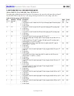
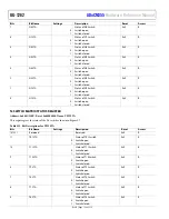
corresponding bit in the INTCFLAGx register is set. The available interrupt sources are shown in Table 173.
CONFIGURING THE INTERRUPTS
The first step to configure the INTC interrupts is to configure the digital die GPIO pin that connects internally to the AFE interrupt
controller output. To configure the GPIO pin, take the following steps:
1.
Configure the internal GPIO2 Pin 1 as a GPIO as follows:
DioCfgPin(pADI_GPIO2, PIN1, 0);
2.
Configure the internal P2.1 pin as an input as follows:
DioIenPin(pADI_GPIO2, PIN1, 1); /* Enable P2.1 input path. */
3.
Enable External Interrupt 3 and configure for falling edge as follows:
EiCfg(EXTINT3, INT_EN, INT_FALL); /* Falling edge. */
4.
Enable the interrupt in the NVIC as follows:
NVIC_EnableIRQ(AFE_EVT3_IRQn);
When these steps are complete, the digital die is configured for INTC interrupts. To configure the AFE INTC interrupts, first write to the
INCT0POL to configure the polarity. To enable the required interrupt, write to the INTCSEL0 register. To clear an interrupt source,
write to the corresponding bit in the INTCCLR register.
CUSTOM INTERRUPTS
Four custom interrupt sources are selectable by the user in the INTCSELx register, Bits[12:9]. For these custom interrupts to generate an
interrupt event, write to the corresponding bit in the AFEGENINTSTA register. It is only possible to write to this register via the sequencer.
Table 173. Interrupt Sources Summary
INTCFLAGx Register Flag Name
Interrupt Source Description
FLAG0
ADC result IRQ status.
FLAG1
DFT result IRQ status.
FLAG2
Sinc2 filter result ready IRQ status.
FLAG3
Temperature result IRQ status.
FLAG4
ADC minimum fail IRQ status.
FLAG5
ADC maximum fail IRQ status.
FLAG6
ADC delta fail IRQ status.
FLAG7
Mean IRQ status.
FLAG13
Bootload done IRQ status.
FLAG15
End of sequence IRQ status.
FLAG16
Sequencer timeout finished IRQ status (see the Timer Command section).
FLAG17
Sequencer timeout command error IRQ status (see the Timer Command section).
FLAG23
Data FIFO full IRQ status.
FLAG24
Data FIFO empty IRQ status.
FLAG25
Data FIFO threshold IRQ status, threshold value set in DATAFIFOTHRES register.
FLAG26
Data FIFO overflow IRQ status.
FLAG27
Data FIFO underflow IRQ status.
FLAG29
Outlier IRQ status, detects when an outlier is detected.
FLAG31
Attempt to break IRQ status. This interrupt is set if a Sequence B request occurs when Sequence A is
running. This interrupt indicates that Sequence B is ignored.


