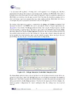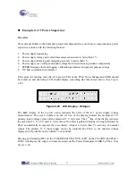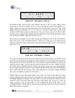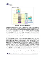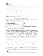
1 is associated with regulator 1. Timing slot 2 with regulator 2 etc. Changing the checkbox
assignments will change the sequence of powering up the regulators on PME EBK. Since rails 2
through 4 derive their input power from the output of regulator 1 (this is a hardwired connection on
PME EBK), we will always need to power up rail 1 first. Therefore, the checkbox assigning rail 1 to
slot 1 will always need to be assigned that way when working with the PME EBK. Feel free to
re-configure the power-up sequence of the other 3 rails (V2 through V4).
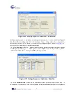
The timing of the power-up sequence is controlled by the
Ramp
and
Up Delay
parameters both
expressed in units of 1 ms (
NOTE:
this unit is customizable. Refer to Cypress application note
AN62496
for more details). The
Ramp
parameter defines how long the Voltage Sequencer should
wait after enabling a regulator before checking for pass or fail on the PGOOD input. The
Up Delay
parameter defines how long the
Voltage Sequencer
should wait once the timing slot has powered-up
successfully before moving on to the next timing slot. This provides external components powered
by the regulator the time needed to power up and initialize properly before moving to the next
power/timing slot. (See
Figure 4-16
below for the correct configuration).
Figure 4-16 Voltage Sequencer Customizer Sequencer Tab
The
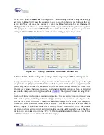
Power Down
pull-down menu control specifies how the regulators should be turned off in case
of fault or system power down. The
All Off
setting sets it to simultaneous shutdown.
Forward
and
Reverse
are 2 other built-in options that enable designers to control the power-down sequence and
timing (controlled by the
Dn Delay
parameter). The chart in the upper part of this tab displays the
current sequencer configuration for visual confirmation that the settings have been entered
correctly.
23
Summary of Contents for CY8CKIT-035
Page 1: ......
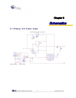
Page 38: ...Chapter 5 Schematics 5 1 Primary 12V Power Input 37 ...
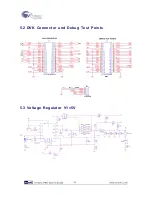
Page 39: ...5 2 DVK Connector and Debug Test Points 5 3 Voltage Regulator V1 5V 38 ...
Page 40: ...5 4 Voltage Regulator V2 3 3V 5 5 Voltage Regulator V3 2 5V 5 6 Voltage Regulator V4 1 8V 39 ...
Page 41: ...5 7 I2C SMBus PMBus Interface Connector 5 8 Layout 5 8 1 Top Layer 40 ...
Page 42: ...5 8 2 Ground Layer 5 8 3 Power Layer 41 ...
Page 43: ...5 8 4 Bottom Layer 42 ...
Page 44: ...5 8 5 Top Silkscreen 43 ...

