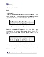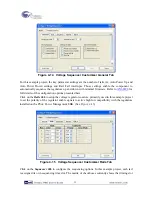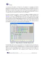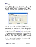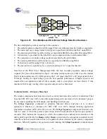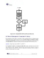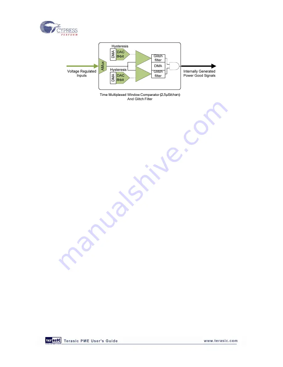
Figure 4-18 Time Multiplexed Over/Under Voltage Detection Hardware
The time-multiplexing works according to this sequence:
1.
The scaled regulator output for rail[n] (signal C[n]) is multiplexed into the window comparator
2.
The under and over voltage limits for rail[n] are copied from SRAM to the DAC using DMA
3.
The previous glitch filter result for rail[n] is copied from SRAM to the glitch filter using DMA
4.
A short delay is provided to allow the DACs and comparators time to settle and stabilize
5.
The comparator over/under voltage results are sampled by the glitch filters
6.
The current glitch filter result for rail[n] is copied back to SRAM using DMA
7.
Connection to rail[n] (signal C[n]) is removed
8.
The next rail[n+1] (signal C[n+1]) is selected and steps 1 to 7 repeat for that rail
Note that on the PSoC Power Management EBK, the four secondary regulator output voltages
(signals C[4:1]) are all normalized to about 1 volt using scaling resistors in order to use the internal
DAC’s fastest update rate of 1,000 ksps using the 1 volt range (the DAC’s 4V range update rate is
250 ksps). Scaling the input voltage gives the best possible performance. If higher speed is not
required for your application, and all the secondary rails in your system are lower than 4 V (the
maximum DAC range), scaling of the regulator outputs can be eliminated.
Technical Details – Firmware Flowchart
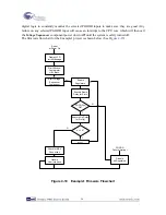
The window comparator fault detection circuit is entirely hardware driven after it is initialized. That
frees the 8051 CPU core 100% to do other application-specific user tasks. In the Example1 project,
the user task is updating the LCD display and handling switch presses.
The
Voltage Sequencer
component is primarily firmware driven, and since it is a critical
system-level function, it consumes the 8051 CPU core 100% through blocking application
programmer interface (API) calls when in use. The
Voltage Sequencer
component firmware only
runs in 2 cases: 1) when the system is powered up at which time the selected power-up sequence is
executed. This includes the sequence in which the regulators are enabled, and execution of the
timing delays specified by the
Ramp
and
Up Delays
entered into the component customizer and 2)
when the system is powered down due to a regulator fault, as detected by the window comparator
hardware. When all regulators are powered on and running, the
Voltage Sequencer
component uses
25
Summary of Contents for CY8CKIT-035
Page 1: ......
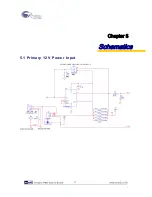
Page 38: ...Chapter 5 Schematics 5 1 Primary 12V Power Input 37 ...
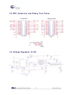
Page 39: ...5 2 DVK Connector and Debug Test Points 5 3 Voltage Regulator V1 5V 38 ...
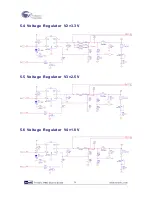
Page 40: ...5 4 Voltage Regulator V2 3 3V 5 5 Voltage Regulator V3 2 5V 5 6 Voltage Regulator V4 1 8V 39 ...
Page 41: ...5 7 I2C SMBus PMBus Interface Connector 5 8 Layout 5 8 1 Top Layer 40 ...
Page 42: ...5 8 2 Ground Layer 5 8 3 Power Layer 41 ...
Page 43: ...5 8 4 Bottom Layer 42 ...
Page 44: ...5 8 5 Top Silkscreen 43 ...

