MSP430FG47x
MIXED SIGNAL MICROCONTROLLER
SLAS580D -- OCTOBER 2008 -- REVISED MARCH 2011
50
POST OFFICE BOX 655303
DALLAS, TEXAS 75265
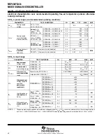
electrical characteristics over recommended operating free-air temperature (unless otherwise
noted)
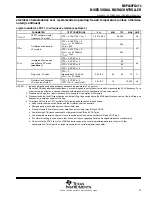
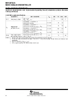
12-bit DAC, reference input specifications
PARAMETER
TEST CONDITIONS
V
CC
MIN
TYP
MAX
UNIT
V
Reference input
DAC12IR = 0 (see Notes 1 and 2)
2.2 V/3 V
AV
CC
/3
AV
CC
+0.2
V
V
REF
Reference input
voltage range
DAC12IR = 1 (see Notes 3 and 4)
2.2 V/3 V
AV
CC
AV
CC
+0.2
V
Ri
(VREF)
Reference input
resistance
DAC12IR = 0, SD16VMIDON = 1
(see Note 5)
2.2 V/3 V
20
M
Ri
(VREF)
resistance
DAC12IR = 1, SD16VMIDON = 1
2.2 V/3 V
40
48
56
k
NOTES: 1. For a full-scale output, the reference input voltage can be as high as 1/3 of the maximum output voltage swing (AV
CC
).
2. The maximum voltage applied at reference input voltage terminal V
REF
= [AV
CC
-- V
E(O)
] / [3*(1 + E
G
)].
3. For a full-scale output, the reference input voltage can be as high as the maximum output voltage swing (AV
CC
).
4. The maximum voltage applied at reference input voltage terminal V
REF
= [AV
CC
-- V
E(O)
] / (1 + E
G
).
5. Characterized, not production tested
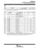
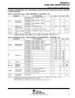
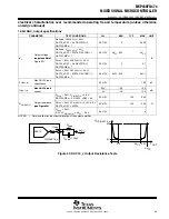
12-bit DAC, dynamic specifications (V
REF,DAC12
= AV
CC
, DAC12IR = 1) (see Figure 24 and Figure 25)
PARAMETER
TEST CONDITIONS
V
CC
MIN
TYP
MAX
UNIT
DAC12
DAC12_xDAT = 800h,
DAC12AMPx = 0
{2, 3, 4}
2.2 V/3 V
60
120
t
ON
DAC12
on time
DAC12_xDAT = 800h,
Error
V(O)
<
0.5 LSB
DAC12AMPx = 0
{5, 6}
2.2 V/3 V
15
30
s
t
ON
on-time
Error
V(O)
<
0.5 LSB
(see Note 1, Figure 24)
DAC12AMPx = 0
7
2.2 V/3 V
6
12
s
Settling
DAC12 xDAT
DAC12AMPx = 2
2.2 V/3 V
100
200
t
S(FS)
Settling
time full scale
DAC12_xDAT =
80h
F7Fh
80h
DAC12AMPx = 3,5
2.2 V/3 V
40
80
s
t
S(FS)
time,full-scale 80h
F7Fh
80h
DAC12AMPx = 4,6,7
2.2 V/3 V
15
30
s
Settling time
DAC12_xDAT =
DAC12AMPx = 2
2.2 V/3 V
5
t
S(C-C)
Settling time,
code to code
DAC12_xDAT =
3F8h
408h
3F8h
DAC12AMPx = 3,5
2.2 V/3 V
2
s
t
S(C-C)
code to code
3F8h
408h
3F8h
BF8h
C08h
BF8h
DAC12AMPx = 4,6,7
2.2 V/3 V
1
s
DAC12 xDAT
DAC12AMPx = 2
2.2 V/3 V
0.05
0.12
SR
Slew Rate
DAC12_xDAT =
80h
F7Fh
80h
DAC12AMPx = 3,5
2.2 V/3 V
0.35
0.7
V/
s
SR
Slew Rate
80h
F7Fh
80h
DAC12AMPx = 4,6,7
2.2 V/3 V
1.5
2.7
V/
s
DAC12 xDAT
DAC12AMPx = 2
2.2 V/3 V
600
Glitch energy: full-scale
DAC12_xDAT =
80h
F7Fh
80h
DAC12AMPx = 3,5
2.2 V/3 V
150
nV-s
Glitch energy: full scale
80h
F7Fh
80h
DAC12AMPx = 4,6,7
2.2 V/3 V
30
nV s
NOTES: 1. R
Load
and C
Load
connected to AV
SS
(not AV
CC
/2) in Figure 24.
2. Slew rate applies to output voltage steps > = 200 mV.
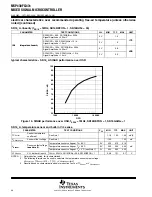
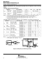
RLoad
AVCC
CLoad = 100pF
2
DAC Output
RO/P(DAC12.x)
ILoad
Conversion 1
Conversion 2
VOUT
Conversion 3
Glitch
Energy
+/-- 1/2 LSB
+/-- 1/2 LSB
tsettleLH
tsettleHL
= 3 k
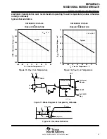
Figure 24. Settling Time and Glitch Energy Testing
Summary of Contents for MSP430FG47x
Page 91: ......

