THCV242_ Rev.2.00_E
Copyright
©
2019 THine Electronics, Inc. THine Electronics, Inc.
32/53
Security E
Header/Packet/Sync Pre-processing
Setting of Header, Packet and Sync pre-processing can be configurable by 2-wire access to internal register.
Settings of Header, Packet and Sync pre-processing exist for each Main-Link input lanes respectively.
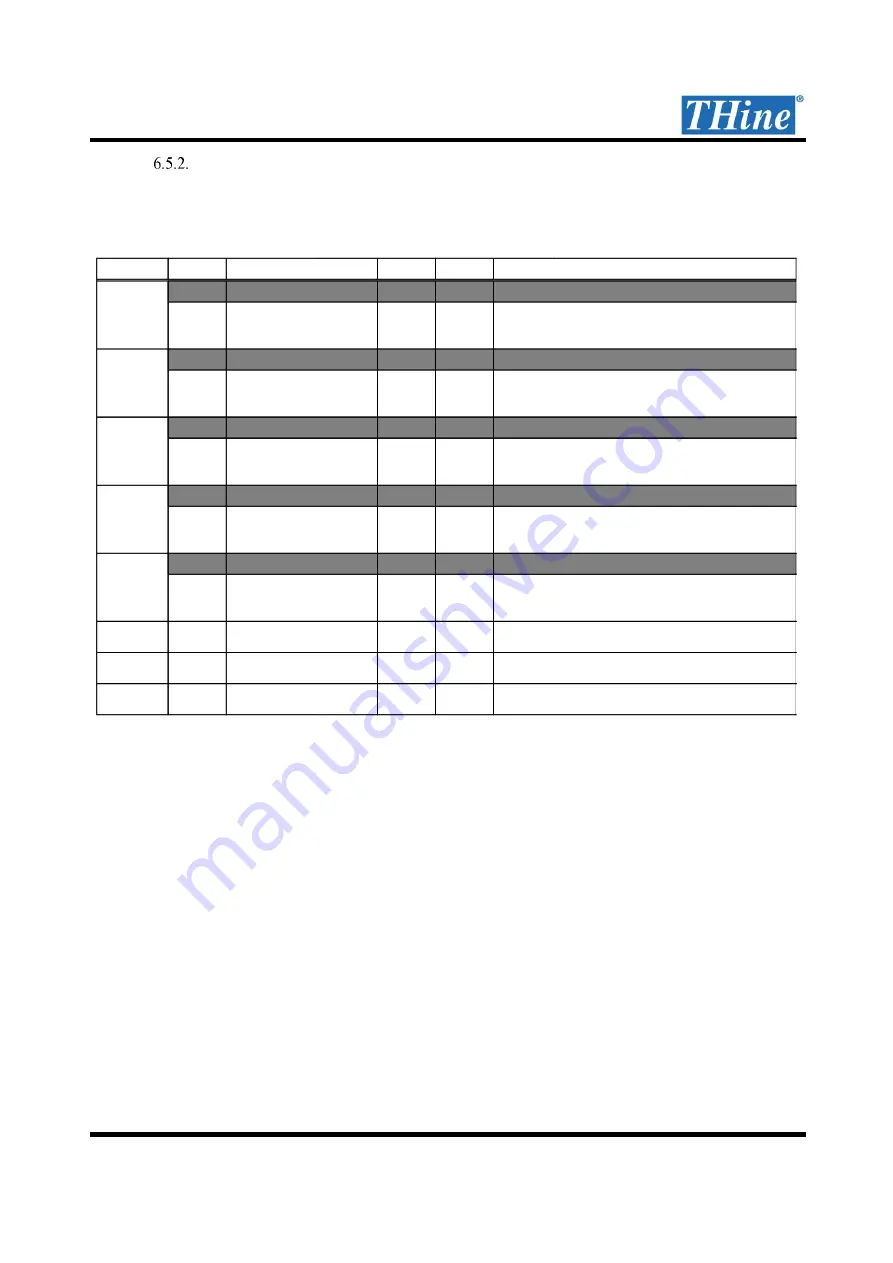
Table 19.
Header/Packet/Sync pre-processing setting for Main-Link Lane0 example
Address
bit
R/W
Initial
0x1100
[7:1]
-
7'h00
[0]
R/W
1'b0
0x1101
[7:1]
-
7'h00
[0]
R/W
1'b0
0x1102
[7:1]
-
7'h00
[0]
R/W
1'b0
0x1103
[7:1]
-
7'h00
[0]
R/W
1'b0
0x1104
[7:1]
-
7'h00
[0]
R/W
1'b0
0x1105
[7:0]
R/W
8'h00
0x1106
[7:0]
R/W
8'h00
0x1107
[7:0]
R/W
8'h00
R_VX1_DATAID0
Main-Link Lane0 to MIPI Data ID manual setting
(Only active when R_VX1_PH_EN=0)
R_VX1_WC_UP0
Main-Link Lane0 to MIPI Word Count (MSB 8bit)
manual setting (Only active when R_VX1_PH_EN=0)
R_VX1_WC_LOW0
Main-Link Lane0 to MIPI Word Count (LSB 8bit)
manual setting (Only active when R_VX1_PH_EN=0)
-
Reserved
R_VX1_VSYNC_POL0
Main-Link Lane0 VSYNC intake polarity
1'b0: Low active / VSYNC=Low pulse
1'b1: High active / VSYNC=High pulse
-
Reserved
R_VX1_VVALID_MODE0
Main-Link Lane0 to MIPI VVALID generation mode
1'b0: mode1 (available with THCV241)
1'b1: mode2 (FS/FE generation from VSYNC)
-
Reserved
R_VX1_SP_EN0
Main-Link Lane0 Input MIPI Short Packet intake
1'b0: Short Packet from Main-Link Lane0 not used
1'b1: Short Packet from Main-Link Lane0 input
-
Reserved
R_VX1_CRC_EN0
Main-Link Lane0 Input CRC intake
1'b0: CRC from Main-Link Lane0 not used
1'b1: CRC from Main-Link Lane0 input
R_VX1_PH_EN0
Main-Link Lane0 Input MIPI Packet Header intake
1'b0: Packet Header from Main-Link Lane0 not used
1'b1: Packet Header from Main-Link Lane0 input
Register Name
Description
-
Reserved


