background image

8 Bit Microcontroller

TLCS-870/C Series

TMP86PM29BUG

Summary of Contents for TLCS-870/C Series

Page 1: ...8 Bit Microcontroller TLCS 870 C Series TMP86PM29BUG ...

Page 2: ...or usage in equipment that requires extraordinarily high quality and or reliability or a malfunction or failure of which may cause loss of human life or bodily injury Unintended Usage Unintended Usage include atomic energy control instruments airplane or spaceship instruments transportation instruments traffic signal instruments combustion control instruments medical instruments all types of safet...

Page 3: ... in data sheet of each product Products name TMP86CM29L TMP86C829B TMP86CH29B TMP86CM29B TMP86CH21 TMP86CH21A TMP86C420 TMP86C820 ROM 32 K bytes C829 8K bytes CH29 16K bytes CM29 32K bytes 16K bytes C420 4K bytes C820 8K bytes RAM 1 5K bytes C829 512bytes CH29 1 5K bytes CM29 1 5K bytes 512bytes 256bytes I O port 39 pins Minumum command execution time 0 25µsec at 16MHz Supply Voltage 1 8V to 3 6V ...

Page 4: ...OM mode in TMP86FM29 is different from MCU mode Fore details please refer to Electirical Characteristics in data sheet of each product Products name TMP86C829B TMP86CH29B TMP86CM29B TMP86PM29A TMP86PM29B TMP86FM29 TMP86CM29L ROM 8K bytes MASK 16K bytes MASK 32K bytes MASK 32K bytes OTP 32K bytes FLASH 32K bytes MASK RAM 512 bytes 1 5K bytes DBR 128 bytes Flash memory control status registers EEPCR...

Page 5: ...ge level of V3 pin always should be under 3 6V Note 2 The operating temperature of TMP86FM29 CM29L in Type 1 and Type 2 is 10 to 85 For details please refer to LCD Driver and Electrical Characteristics in data sheet Note 3 The operating temperature of TMP86C829B CH29B CM29B in all Types Type 1 to 5 is 40 to 85 However there is a voltage level limitation of V3 and VDD pin in each type For details p...

Page 6: ...TMP86PM29BUG ...

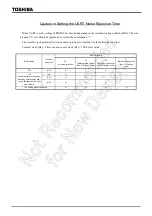
Page 7: ...Revision History Date Revision 2007 10 11 1 First Release 2008 8 29 2 Contents Revised ...

Page 8: ...ted by the following equation Transfer clock Hz Timer counter source clock Hz TTREG set value BRG setting Transfer clock Hz RXDNC setting 00 No noise rejection 01 Reject pulses shorter than 31 fc s as noise 10 Reject pulses shorter than 63 fc s as noise 11 Reject pulses shorter than 127 fc s as noise 000 fc 13 O O O 110 When the transfer clock gen erated by timer counter inter rupt is the same as ...

Page 9: ......

Page 10: ...2 4 Operating Mode Control 18 2 2 4 1 STOP mode 2 2 4 2 IDLE1 2 mode and SLEEP1 2 mode 2 2 4 3 IDLE0 and SLEEP0 modes IDLE0 SLEEP0 2 2 4 4 SLOW mode 2 3 Reset Circuit 31 2 3 1 External Reset Input 31 2 3 2 Address trap reset 32 2 3 3 Watchdog timer reset 32 2 3 4 System clock reset 32 3 Interrupt Control Circuit 3 1 Interrupt latches IL15 to IL2 35 3 2 Interrupt enable register EIR 36 3 2 1 Interr...

Page 11: ...70 58 6 Watchdog Timer WDT 6 1 Watchdog Timer Configuration 59 6 2 Watchdog Timer Control 60 6 2 1 Malfunction Detection Methods Using the Watchdog Timer 60 6 2 2 Watchdog Timer Enable 61 6 2 3 Watchdog Timer Disable 62 6 2 4 Watchdog Timer Interrupt INTWDT 62 6 2 5 Watchdog Timer Reset 63 6 3 Address Trap 64 6 3 1 Selection of Address Trap in Internal RAM ATAS 64 6 3 2 Selection of Operation at A...

Page 12: ... 2 High Frequency Warm Up Counter Mode SLOW1 SLOW2 NORMAL2 NORMAL1 10 8 Bit TimerCounter TC5 TC6 10 1 Configuration 101 10 2 TimerCounter Control 102 10 3 Function 106 10 3 1 8 Bit Timer Mode TC5 and 6 106 10 3 2 8 Bit Event Counter Mode TC6 107 10 3 3 8 Bit Programmable Divider Output PDO Mode TC6 107 10 3 4 8 Bit Pulse Width Modulation PWM Output Mode TC6 110 10 3 5 16 Bit Timer Mode TC5 and 6 1...

Page 13: ...35 12 6 Transfer Mode 136 12 6 1 4 bit and 8 bit transfer modes 136 12 6 2 4 bit and 8 bit receive modes 138 12 6 3 8 bit transfer receive mode 139 13 10 bit AD Converter ADC 13 1 Configuration 141 13 2 Register configuration 142 13 3 Function 145 13 3 1 Software Start Mode 145 13 3 2 Repeat Mode 145 13 3 3 Register Setting 146 13 4 STOP SLOW Modes during AD Conversion 147 13 5 Analog Input Voltag...

Page 14: ...eed program writing 16 1 2 2 Program Writing using a General purpose PROM Programmer 17 Input Ouput Circuitry 17 1 Control Pins 175 17 2 Input Output Ports 176 18 Electrical Characteristics 18 1 Absolute Maximum Ratings 177 18 2 Recommended Operating Condition 178 18 3 DC Characteristics 179 18 4 AD Conversion Characteristics 180 18 5 AC Characteristics 181 18 6 Timer Counter 1 input ECIN Characte...

Page 15: ...vi ...

Page 16: ...OSHIBA products listed in this document shall be made at the customer s own risk 021023_B The products described in this document shall not be used or embedded to any downstream products of which manufacture use and or sale are prohibited under any applicable laws and regulations 060106_Q The information contained herein is presented only as a guide for the applications of our products No responsi...

Page 17: ...g low frequency clock High frequency clock oscillate IDLE0 mode CPU stops and only the Time Based Timer TBT on peripherals operate using high fre quency clock Release by falling edge of the source clock which is set by TBTCR TBTCK IDLE1 mode CPU stops and peripherals operate using high frequency clock Release by interru puts CPU restarts IDLE2 mode CPU stops and peripherals operate using high and ...

Page 18: ... 21 20 19 18 17 49 50 51 52 53 54 55 56 57 58 59 60 61 62 63 64 P15 SEG26 RXD SI P17 SEG24 SCK P50 SEG23 P52 SEG21 P51 SEG22 P54 SEG19 P53 SEG20 P16 SEG25 TXD SO SEG3 SEG4 SEG5 SEG6 SEG7 P77 SEG8 P76 SEG9 P75 SEG10 ECIN AIN1 P61 XIN P67 AIN7 STOP5 AVDD P10 SEG31 P11 SEG30 P14 SEG27 INT3 P12 SEG29 INT1 VAREF P13 SEG28 INT2 P74 SEG11 P73 SEG12 P72 SEG13 P71 SEG14 P70 SEG15 P57 SEG16 P56 SEG17 P55 SE...

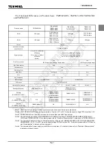
Page 19: ...Page 4 1 3 Block Diagram TMP86PM29BUG 1 3 Block Diagram Figure 1 2 Block Diagram ...

Page 20: ... P13 SEG28 INT2 23 IO I I PORT13 LCD segment output 28 External interrupt 2 input P12 SEG29 INT1 22 IO O I PORT12 LCD segment output 29 External interrupt 1 input P11 SEG30 21 IO O PORT11 LCD segment output 30 P10 SEG31 20 IO O PORT10 LCD segment output 31 P22 XTOUT 7 IO O PORT22 Resonator connecting pins 32 768kHz for inputting external clock P21 XTIN 6 IO I PORT21 Resonator connecting pins 32 76...

Page 21: ...65 AIN5 STOP3 15 IO I I PORT65 Analog Input5 STOP3 input P64 AIN4 STOP2 14 IO I I PORT64 Analog Input4 STOP2 input P63 AIN3 INT0 13 IO I I PORT63 Analog Input3 External interrupt 0 input P62 AIN2 ECNT 12 IO I I PORT62 Analog Input2 ECNT input P61 AIN1 ECIN 11 IO I I PORT61 Analog Input1 ECIN input P60 AIN0 10 IO I PORT60 Analog Input0 P77 SEG8 43 IO O PORT77 LCD segment output 8 P76 SEG9 42 IO O P...

Page 22: ...1 54 O LCD common output 1 COM0 55 O LCD common output 0 V3 56 I LCD voltage booster pin V2 57 I LCD voltage booster pin V1 58 I LCD voltage booster pin C1 59 I LCD voltage booster pin C0 60 I LCD voltage booster pin XIN 2 I Resonator connecting pins for high frequency clock XOUT 3 O Resonator connecting pins for high frequency clock RESET 8 IO Reset signal TEST 4 I Test pin for out going test Nor...

Page 23: ...Page 8 1 4 Pin Names and Functions TMP86PM29BUG ...

Page 24: ...ogram memory OTP 2 1 3 Data Memory RAM The TMP86PM29BUG has 1536bytes Address 0040H to 063FH of internal RAM The first 192 bytes 0040H to 00FFH of the internal RAM are located in the direct area instructions with shorten operations are available against such an area SFR 0000H 64 bytes SFR RAM Special function register includes I O ports Peripheral control registers Peripheral status registers Syst...

Page 25: ...sumption can be reduced by switching of the standby controller to low power operation based on the low frequency clock The high frequency fc clock and low frequency fs clock can easily be obtained by connecting a resonator between the XIN XOUT and XTIN XTOUT pins respectively Clock input from an external oscillator is also possible In this case external clock is applied to XIN XTIN pin with XOUT X...

Page 26: ... oscillation frequency can be adjusted by monitoring the pulse which the fixed frequency is outputted to the port by the program The system to require the adjustment of the oscillation frequency should create the program for the adjust ment in advance XOUT XIN Open XOUT XIN XTOUT XTIN Open XTOUT XTIN a Crystal Ceramic resonator b External oscillator c Crystal d External oscillator High frequency c...

Page 27: ...Configuration of timing generator The timing generator consists of a 2 stage prescaler a 21 stage divider a main system clock generator and machine cycle counters An input clock to the 7th stage of the divider depends on the operating mode SYSCR2 SYSCK and TBTCR DV7CK that is shown in Figure 2 4 As reset and STOP mode started canceled the prescaler and the divider are cleared to 0 Figure 2 4 Confi...

Page 28: ... 4 states S0 to S3 and each state consists of one main system clock Figure 2 5 Machine Cycle 2 2 3 Operation Mode Control Circuit The operation mode control circuit starts and stops the oscillation circuits for the high frequency and low frequency clocks and switches the main system clock There are three operating modes Single clock mode dual clock mode and STOP mode These modes are controlled by ...

Page 29: ...rrupt individual enable flag 1 and TBTCR TBTEN 1 interrupt pro cessing is performed When IDLE0 mode is entered while TBTCR TBTEN 1 the INTTBT interrupt latch is set after returning to NORMAL1 mode 2 2 3 2 Dual clock mode Both the high frequency and low frequency oscillation circuits are used in this mode P21 XTIN and P22 XTOUT pins cannot be used as input output ports The main system clock is obta...

Page 30: ...r the SLEEP1 mode except for the oscillation circuit of the high frequency clock 7 SLEEP0 mode In this mode all the circuit except oscillator and the timer base timer stops operation This mode is enabled by setting 1 on bit SYSCR2 TGHALT When SLEEP0 mode starts the CPU stops and the timing generator stops feeding the clock to the peripheral circuits other than TBT Then upon detecting the falling e...

Page 31: ...te Operate Operate IDLE1 Halt IDLE0 Halt STOP Stop Halt Dual clock NORMAL2 Oscillation Oscillation Operate with high frequency Operate Operate 4 fc s IDLE2 Halt SLOW2 Operate with low frequency 4 fs s SLEEP2 Halt SLOW1 Stop Operate with low frequency SLEEP1 Halt SLEEP0 Halt STOP Stop Halt Note 2 SYSCR2 XEN 1 STOP pin input STOP pin input STOP pin input Interrupt Interrupt SYSCR2 XEN 0 SYSCR2 SYSCK...

Page 32: ... SLEEP0 mode is released TGHALT is automatically cleared to 0 Note 8 Before setting TGHALT to 1 be sure to stop peripherals If peripherals are not stopped the interrupt latch of peripherals may be set after IDLE0 or SLEEP0 mode is released System Control Register 1 SYSCR1 7 6 5 4 3 2 1 0 0038H STOP RELM RETM OUTEN WUT Initial value 0000 00 STOP STOP mode start 0 CPU core and peripherals remain act...

Page 33: ... the release input the STOP pin must be used for releasing STOP mode Note 2 During STOP period from start of STOP mode to end of warm up due to changes in the external interrupt pin signal interrupt latches may be set to 1 and interrupts may be accepted immediately after STOP mode is released Before starting STOP mode therefore disable interrupts Also before enabling interrupts after STOP mode is ...

Page 34: ... any STOP5 to STOP2 pin input for releasing STOP mode in edge sensitive release mode Figure 2 8 Edge sensitive Release Mode Example 2 Starting STOP mode from NORMAL mode with an INT5 interrupt PINT5 TEST P2PRD 0 To reject noise STOP mode does not start if JRS F SINT5 port P20 is at high LD SYSCR1 01010000B Sets up the level sensitive release mode DI IMF 0 SET SYSCR1 7 Starts STOP mode SINT5 RETI E...

Page 35: ...ng low level on the RESET pin which immediately performs the normal reset operation Note 3 When STOP mode is released with a low hold voltage the following cautions must be observed The power supply voltage must be at the operating voltage level before releasing STOP mode The RESET pin input must also be H level rising together with the power supply voltage In this case if an external time constan...

Page 36: ...ode start Example Start with SET SYSCR1 7 instruction located at address a a 6 a 5 a 4 a 3 a 2 n 2 n 3 n 4 a 3 n 1 Instruction address a 2 2 1 0 3 b STOP mode release Count up Turn off Halt Oscillator circuit Program counter Instruction execution Divider Main system clock Oscillator circuit STOP pin input Program counter Instruction execution Divider Main system clock ...

Page 37: ...ate 2 The data memory CPU registers program status word and port output latches are all held in the status in effect before these modes were entered 3 The program counter holds the address 2 ahead of the instruction which starts these modes Figure 2 10 IDLE1 2 and SLEEP1 2 Modes Reset Reset input 0 1 Interrupt release mode Yes No No CPU and WDT are halted Interrupt request IMF Interrupt processing...

Page 38: ...al release mode IMF 0 IDLE1 2 and SLEEP1 2 modes are released by any interrupt source enabled by the individual interrupt enable flag EF After the interrupt is generated the program operation is resumed from the instruction following the IDLE1 2 and SLEEP1 2 modes start instruction Normally the interrupt latches IL of the interrupt source used for releasing must be cleared to 0 by load instruction...

Page 39: ...interrupt 㽲㩷Normal release mode 㽳㩷Interrupt release mode Main system clock Interrupt request Program counter Instruction execution Watchdog timer Main system clock Interrupt request Program counter Instruction execution Watchdog timer Main system clock Interrupt request Program counter Instruction execution Watchdog timer a IDLE1 2 and SLEEP1 2 modes start Example Starting with the SET instruction...

Page 40: ... before IDLE0 and SLEEP0 modes were entered 3 The program counter holds the address 2 ahead of the instruction which starts IDLE0 and SLEEP0 modes Note Before starting IDLE0 or SLEEP0 mode be sure to stop Disable peripherals Figure 2 12 IDLE0 and SLEEP0 Modes Yes Normal release mode Yes Interrupt release mode No Yes Reset input CPU and WDT are halted Reset TBT source clock falling edge TBTCR TBTEN...

Page 41: ...de Note IDLE0 and SLEEP0 modes start release without reference to TBTCR TBTEN setting 1 Normal release mode IMF EF6 TBTCR TBTEN 0 IDLE0 and SLEEP0 modes are released by the source clock falling edge which is setting by the TBTCR TBTCK After the falling edge is detected the program operation is resumed from the instruction following the IDLE0 and SLEEP0 modes start instruction Before starting the I...

Page 42: ...pt release mode Main system clock Interrupt request Program counter Instruction execution Watchdog timer Main system clock TBT clock TBT clock Program counter Instruction execution Watchdog timer Main system clock Program counter Instruction execution Watchdog timer a 3 a 2 a 4 a 3 a 3 a IDLE0 and SLEEP0 modes start Example Starting with the SET instruction located at address a b IDLE and SLEEP0 m...

Page 43: ...hing from SLOW mode to stop mode Example 1 Switching from NORMAL2 mode to SLOW1 mode SET SYSCR2 5 SYSCR2 SYSCK 1 Switches the main system clock to the low frequency clock for SLOW2 CLR SYSCR2 7 SYSCR2 XEN 0 Turns off high frequency oscillation Example 2 Switching to the SLOW1 mode after low frequency clock has stabilized SET SYSCR2 6 SYSCR2 XTEN 1 LD TC3CR 43H Sets mode for TC4 3 16 bit mode fs fo...

Page 44: ... by inputting low level on the RESET pin After releasing reset the operation mode is started from NORMAL1 mode Example Switching from the SLOW1 mode to the NORMAL2 mode fc 16 MHz warm up time is 4 0 ms SET SYSCR2 7 SYSCR2 XEN 1 Starts high frequency oscillation LD TC3CR 63H Sets mode for TC4 3 16 bit mode fc for source LD TC4CR 05H Sets warming up counter mode LD TTREG4 0F8H Sets warm up time DI I...

Page 45: ...LR SYSCR2 7 SET SYSCR2 5 NORMAL2 mode Turn off a Switching to the SLOW mode SLOW1 mode SLOW2 mode CLR SYSCR2 5 b Switching to the NORMAL2 mode High frequency clock Low frequency clock Main system clock Instruction execution SYSCK XEN High frequency clock Low frequency clock Main system clock Instruction execution SYSCK XEN SLOW1 mode Warm up during SLOW2 mode ...

Page 46: ...wer supply volt age within the operating voltage range and oscillation stable a reset is applied and the internal state is initial ized When the RESET pin input goes high the reset operation is released and the program execution starts at the vector address stored at addresses FFFEH to FFFFH Figure 2 15 Reset Circuit Table 2 3 Initializing Internal Status by Reset Action On chip Hardware Initial V...

Page 47: ... address r is fetched and decoded Note 3 Varies on account of external condition voltage or capacitance Figure 2 16 Address Trap Reset 2 3 3 Watchdog timer reset Refer to Section Watchdog Timer 2 3 4 System clock reset If the condition as follows is detected the system clock reset occurs automatically to prevent dead lock of the CPU The oscillation is continued without stopping In case of clearing...

Page 48: ...Page 33 TMP86PM29BUG ...

Page 49: ...Page 34 2 Operational Description 2 3 Reset Circuit TMP86PM29BUG ...

Page 50: ...enerated the latch is set to 1 and the CPU is requested to accept the interrupt if its interrupt is enabled The interrupt latch is cleared to 0 immediately after accepting inter rupt All interrupt latches are initialized to 0 during reset The interrupt latches are located on address 003CH and 003DH in SFR area Each latch can be cleared to 0 indi vidually by instruction However IL2 and IL3 should n...

Page 51: ... IMF 0 all maskable interrupts are not accepted regardless of the status on each individual interrupt enable flag EF By setting IMF to 1 the interrupt becomes acceptable if the individuals are enabled When an interrupt is accepted IMF is cleared to 0 after the latest status on IMF is stacked Thus the maskable inter rupts which follow are disabled By executing return interrupt instruction RETI RETN...

Page 52: ...pulat ing EF or IL should be executed before setting IMF 1 Example 1 Enables interrupts individually and sets IMF DI IMF 0 LDW EIRL 1110100010100000B EF15 to EF13 EF11 EF7 EF5 1 Note IMF should not be set EI IMF 1 Example 2 C compiler description example unsigned int _io 3AH EIRL 3AH shows EIRL address _DI EIRL 10100000B _EI ...

Page 53: ...nstruction Then set IMF newly again as required after operating on the EF or IL Enable interrupt by EI instruction In interrupt service routine because the IMF becomes 0 automatically clearing IMF need not execute normally on inter rupt service routine However if using multiple interrupt on interrupt service routine manipulating EF or IL should be exe cuted before setting IMF 1 Interrupt Latches I...

Page 54: ...ruction The interrupt service task terminates upon execution of an interrupt return instruction RETI for maskable interrupts or RETN for non maskable interrupts Figure 3 1 shows the timing chart of interrupt acceptance processing 3 4 1 Interrupt acceptance processing is packaged as follows a The interrupt master enable flag IMF is cleared to 0 in order to disable the acceptance of any fol lowing i...

Page 55: ...upt enable flags To avoid overloaded nesting clear the individual interrupt enable flag whose interrupt is currently serviced before setting IMF to 1 As for non maskable interrupt keep interrupt service shorten compared with length between interrupt requests otherwise the status cannot be recovered as non maskable interrupt would simply nested 3 4 2 Saving restoring general purpose registers Durin...

Page 56: ...terrupts data transfer instructions are available Example Save store register using PUSH and POP instructions PINTxx PUSH WA Save WA register interrupt processing POP WA Restore WA register RETI RETURN Example Save store register using data transfer instructions PINTxx LD GSAVA A Save A register interrupt processing LD A GSAVA Restore A register RETI RETURN PCL PCH PSW At acceptance of an interrup...

Page 57: ...ng executed Thus the next inter rupt can be accepted immediately after the interrupt return instruction is executed RETI RETN Interrupt Return 1 Program counter PC and program status word PSW includes IMF are restored from the stack 2 Stack pointer SP is incremented by 3 Example 1 Returning from address trap interrupt INTATRAP service program PINTxx POP WA Recover SP by 2 LD WA Return Address PUSH...

Page 58: ...terrupt INTUNDEF Taking code which is not defined as authorized instruction for instruction causes INTUNDEF INTUNDEF is gen erated when the CPU fetches such a code and tries to execute it INTUNDEF is accepted even if non maskable inter rupt is in process Contemporary process is broken and INTUNDEF interrupt process starts soon after it is requested Note The undefined instruction interrupt INTUNDEF...

Page 59: ...gnals INT1 INT1 IMF EF5 1 Falling edge or Rising edge Pulses of less than 15 fc or 63 fc s are elimi nated as noise Pulses of 49 fc or 193 fc s or more are considered to be signals In the SLOW or the SLEEP mode pulses of less than 1 fs s are eliminated as noise Pulses of 3 5 fs s or more are considered to be signals INT2 INT2 IMF EF7 1 Falling edge or Rising edge Pulses of less than 7 fc s are eli...

Page 60: ...until a noise reject time is changed is 26 fc External Interrupt Control Register EINTCR 7 6 5 4 3 2 1 0 0037H INT1NC INT0EN INT3ES INT2ES INT1ES Initial value 00 000 INT1NC Noise reject time select 0 Pulses of less than 63 fc s are eliminated as noise 1 Pulses of less than 15 fc s are eliminated as noise R W INT0EN P63 INT0 pin configuration 0 P63 input output port 1 INT0 pin Port P63 should be s...

Page 61: ...Page 46 3 Interrupt Control Circuit 3 8 External Interrupts TMP86PM29BUG ...

Page 62: ...ion register SFR and data buffer register DBR for TMP86PM29BUG 4 1 SFR Address Read Write 0000H Reserved 0001H P1DR 0002H P2DR 0003H P3DR 0004H P3OUTCR 0005H P5DR 0006H P6DR 0007H P7DR 0008H P1PRD 0009H P2PRD 000AH P3PRD 000BH P5PRD 000CH P6CR 000DH P7PRD 000EH ADCCR1 000FH ADCCR2 0010H TREG1AL 0011H TREG1AM 0012H TREG1AH 0013H TREG1B 0014H TC1CR1 0015H TC1CR2 0016H TC1SR 0017H Reserved 0018H TC3C...

Page 63: ...ulation instructions such as SET CLR etc and logical operation instructions such as AND OR etc 0026H UARTCR2 0027H Reserved 0028H LCDCR 0029H P1LCR 002AH P5LCR 002BH P7LCR 002CH PWREG3 002DH PWREG4 002EH PWREG5 002FH PWREG6 0030H Reserved 0031H Reserved 0032H Reserved 0033H Reserved 0034H WDTCR1 0035H WDTCR2 0036H TBTCR 0037H EINTCR 0038H SYSCR1 0039H SYSCR2 003AH EIRL 003BH EIRH 003CH ILL 003DH I...

Page 64: ... 20 0F8BH SEG23 22 0F8CH SEG25 24 0F8DH SEG27 26 0F8EH SEG29 28 0F8FH SEG31 30 0F90H SIOBR0 0F91H SIOBR1 0F92H SIOBR2 0F93H SIOBR3 0F94H SIOBR4 0F95H SIOBR5 0F96H SIOBR6 0F97H SIOBR7 0F98H SIOCR1 0F99H SIOSR SIOCR2 0F9AH STOPCR 0F9BH RDBUF TDBUF 0F9CH Reserved 0F9DH Reserved 0F9EH Reserved 0F9FH Reserved Address Read Write 0FA0H Reserved 0FBFH Reserved Address Read Write 0FC0H Reserved 0FDFH Reser...

Page 65: ...2 DBR TMP86PM29BUG Note 2 Cannot be accessed Note 3 Write only registers and interrupt latches cannot use the read modify write instructions Bit manipulation instructions such as SET CLR etc and logical operation instructions such as AND OR etc ...

Page 66: ...g must be processed by the pro gram Output data changes in the S2 state of the write cycle during execution of the instruction which writes to an I O port Note The positions of the read and write cycles may vary depending on the instruction Figure 5 1 Input Output Timing Example Primary Function Secondary Functions Port P1 8 bit I O port External interrupt input serial interface input output UART ...

Page 67: ...d to 1 P1 port output latch P1DR and P1 port terminal input P1PRD are located on their respective address When read the output latch data the P1DR should be read and when read the terminal input data the P1PRD reg ister should be read If the terminal input data which is configured as LCD segment output is read unstable data is read Figure 5 2 Port P1 Port P1 control register P1DR 0001H R W 7 6 5 4...

Page 68: ...d as an external interrupt input a STOP mode release signal input or an input port If it is used as an output port the interrupt latch is set on the falling edge of the output pulse P2 port output latch P2DR and P2 port terminal input P2PRD are located on their respective address When read the output latch data the P2DR should be read and when read the terminal input data the P2PRD reg ister shoul...

Page 69: ...spective output control P3OUTCR should be set to 0 after P3DR is set to 1 During reset the P3DR is initialized to 1 and the P3OUTCR is initialized to 0 P3 port output latch P3DR and P3 port terminal input P3PRD are located on their respective address When read the output latch data the P3DR should be read and when read the terminal input data the P3PRD reg ister should be read If a read instructio...

Page 70: ...on their respective address When read the output latch data the P5DR should be read and when read the terminal input data the P5PRD reg ister should be read If the terminal input data which is configured as LCD segment output is read unstable data is read Figure 5 5 Port P5 Port P5 control register P5DR 0005H R W 7 6 5 4 3 2 1 0 P57 SEG16 P56 SEG17 P55 SEG18 P54 SEG19 P53 SEG20 P52 SEG21 P51 SEG22...

Page 71: ...P6DR to 1 and P6CR to 0 To use it as an output port set data of P6CR to 1 To use it as an analog input set data of P6DR to 0 and P6CR to 0 and start the AD It is the penetration electric current measures by the analog voltage Pins not used for analog input can be used as I O ports During AD conversion output instructions should not be executed to keep a precision In addition a variable signal shou...

Page 72: ...tructions cannot be used Read modify write instruction writes the all data of 8 bit after data is read and modified Because a bit setting Input mode read data of terminal the output latch is changed by these instruction So P6 port can not input data Port P6 control register P6DR 0006H R W 7 6 5 4 3 2 1 0 P67 AIN7 STOP5 P66 AIN6 STOP4 P65 AIN5 STOP3 P64 AIN4 STOP2 P63 AIN3 INT0 P62 AIN2 ECNT P61 AI...

Page 73: ...t P7PRD are located on their respective address When read the output latch data the P7DR should be read and when read the terminal input data the P7PRD reg ister should be read If the terminal input data which is configured as LCD segment output is read unstable data is read Figure 5 7 Port P7 Port P7 control register P7DR 0007H R W 7 6 5 4 3 2 1 0 P77 SEG8 P76 SEG9 P75 SEG10 P74 SEG11 P73 SEG12 P...

Page 74: ...t used to detect malfunctions it can be used as the timer to provide a periodic inter rupt Note Care must be taken in system design since the watchdog timer functions are not be operated completely due to effect of disturbing noise 6 1 Watchdog Timer Configuration Figure 6 1 Watchdog Timer Configuration 0034H Overflow WDT output Internal reset Binary counters WDTOUT Writing clear code Writing disa...

Page 75: ...og timer interrupt INTWDT is generated The watchdog timer temporarily stops counting in the STOP mode including the warm up or IDLE SLEEP mode and automatically restarts continues counting when the STOP IDLE SLEEP mode is inactivated Note The watchdog timer consists of an internal divider and a two stage binary counter When the clear code 4EH is written only the binary counter is cleared but not t...

Page 76: ...a cycle shorter than 3 4 of the time set in WDTCR1 WDTT 6 2 2 Watchdog Timer Enable Setting WDTCR1 WDTEN to 1 enables the watchdog timer Since WDTCR1 WDTEN is initialized to 1 during reset the watchdog timer is enabled automatically after the reset release Watchdog Timer Control Register 1 WDTCR1 0034H 7 6 5 4 3 2 1 0 ATAS ATOUT WDTEN WDTT WDTOUT Initial value 11 1001 WDTEN Watchdog timer enable d...

Page 77: ... flag IMF When a watchdog timer interrupt is generated while the other interrupt including a watchdog timer interrupt is already accepted the new watchdog timer interrupt is processed immediately and the previous interrupt is held pending Therefore if watchdog timer interrupts are generated continuously without execution of the RETN instruction too many levels of nesting may cause a malfunction of...

Page 78: ... reset is generated in the SLOW1 mode the reset time is maximum 24 fc high fre quency clock since the high frequency clock oscillator is restarted However when crystals have inaccura cies upon start of the high frequency clock oscillator the reset time should be considered as an approximate value because it has slight errors Figure 6 2 Watchdog Timer Interrupt Reset Clock Binary counter Overflow I...

Page 79: ...upt is a non maskable interrupt which can be accepted regardless of the interrupt mas ter flag IMF When an address trap interrupt is generated while the other interrupt including an address trap interrupt is already accepted the new address trap is processed immediately and the previous interrupt is held pending Therefore if address trap interrupts are generated continuously without execution of t...

Page 80: ...et request is generated the RESET pin outputs a low level signal and the internal hardware is reset The reset time is maximum 24 fc s 1 5 µs fc 16 0 MHz Note When an address trap reset is generated in the SLOW1 mode the reset time is maximum 24 fc high fre quency clock since the high frequency clock oscillator is restarted However when crystals have inaccura cies upon start of the high frequency c...

Page 81: ...Page 66 6 Watchdog Timer WDT 6 3 Address Trap TMP86PM29BUG ...

Page 82: ... TBTCR 0036H DVOEN DVOCK DV7CK TBTEN TBTCK Initial Value 0000 0000 TBTEN Time Base Timer enable disable 0 Disable 1 Enable TBTCK Time Base Timer interrupt Frequency select Hz NORMAL1 2 IDLE1 2 Mode SLOW1 2 SLEEP1 2 Mode R W DV7CK 0 DV7CK 1 000 fc 223 fs 215 fs 215 001 fc 221 fs 213 fs 213 010 fc 216 fs 28 011 fc 214 fs 26 100 fc 213 fs 25 101 fc 212 fs 24 110 fc 211 fs 23 111 fc 29 fs 2 fc 223 or ...

Page 83: ... The divider is not cleared by the program therefore only the first interrupt may be generated ahead of the set interrupt period Figure 7 2 Figure 7 2 Time Base Timer Interrupt Example Set the time base timer frequency to fc 216 Hz and enable an INTTBT interrupt LD TBTCR 00000010B TBTCK 010 LD TBTCR 00001010B TBTEN 1 DI IMF 0 SET EIRL 6 Table 7 1 Time Base Timer Interrupt Frequency Example fc 16 0...

Page 84: ...m enabled DVOEN 1 to disable DVOEN 0 do not change the setting of the divider output frequency Time Base Timer Control Register 7 6 5 4 3 2 1 0 TBTCR 0036H DVOEN DVOCK DV7CK TBTEN TBTCK Initial value 0000 0000 DVOEN Divider output enable disable 0 Disable 1 Enable R W DVOCK Divider Output DVO frequency selection Hz NORMAL1 2 IDLE1 2 Mode SLOW1 2 SLEEP1 2 Mode R W DV7CK 0 DV7CK 1 00 fc 213 fs 25 fs...

Page 85: ...00000000B DVOCK 00 LD TBTCR 10000000B DVOEN 1 Table 7 2 Divider Output Frequency Example fc 16 0 MHz fs 32 768 kHz DVOCK Divider Output Frequency Hz NORMAL1 2 IDLE1 2 Mode SLOW1 2 SLEEP1 2 Mode DV7CK 0 DV7CK 1 00 1 953 k 1 024 k 1 024 k 01 3 906 k 2 048 k 2 048 k 10 7 813 k 4 096 k 4 096 k 11 15 625 k 8 192 k 8 192 k ...

Page 86: ... 18 bit up counter Edge detector 10 11 00 S Y Y Pin ECNT Pin CLEAR signal ECIN Pin WGPSCK TC1M SGEDG INTTC1 2 3 2 2 1 1 2 1 2 1 WGPSCK SGEDG SGP SEG TC1C TC1S TC1M TC1CK 2 1 1 1 1 SEG 1 Pulse width measurement mode Frequency measurement mode Timer Event count modes P33 TC6OUT TC6OUT fc 2 12 or fs 2 4 fc 2 13 or fs 2 5 fc 2 14 or fs 2 6 fs 2 15 or fc 2 23 fs 2 5 or fc 2 13 fs 2 3 or fc 2 11 fc 2 7 ...

Page 87: ...AM Initial value 0000 0000 7 6 5 4 3 2 1 0 TREG1AL 0010H R W TREG1AL Initial value 0000 0000 7 6 5 4 3 2 1 0 TREG1B 0013H Ta Tb Initial value 0000 0000 WGPSCK NORMAL1 2 IDLE1 2 modes SLOW1 2 SLEEP1 2 modes R W DV7CK 0 DV7CK 1 Ta Setting H level period of the window gate pulse 00 01 10 16 Ta 212 fc 16 Ta 213 fc 16 Ta 214 fc 16 Ta 24 fs 16 Ta 25 fs 16 Ta 26 fs 16 Ta 24 fs 16 Ta 25 fs 16 Ta 26 fs Tb ...

Page 88: ...lect to internal clock Note 8 When using the event counter mode set TC1CK TC1 source clock select to external clock Note 9 Because the read value is different from the written value do not use read modify write instructions to TREG1A Note 10 fc 27 fc 23can not be used as source clock in SLOW SLEEP mode Note 11 The read data of bits 7 to 2 in TREG1AH are always 0 Data 1 can not be written Timer cou...

Page 89: ...GPSCK TC6OUT 0 Initial value 0000 000 SEG External input clock ECIN edge select 0 1 Counts at the falling edge Counts at the both falling rising edges R W SGP Window gate pulse select 00 01 10 11 ECNT input Internal window gate pulse TREG1B PWM6 PDO6 PPG6 TC6 output Reserved R W SGEDG Window gate pulse interrupt edge select 0 1 Interrupts at the falling edge Interrupts at the falling rising edges ...

Page 90: ...s 7 makes interrupts TC1 status register TC1SR 0016H 7 6 5 4 3 2 1 0 HECF HEOVF 0 0 0 0 0 0 Initial value 0000 0000 HECF Operating Status monitor 0 1 Stop during Tb or disable Under counting during Ta Read only HEOVF Counter overflow monitor 0 1 No overflow Overflow status Table 8 1 Source clock internal clock of Timer Counter 1 Source Clock Resolution Maximum Time Setting NORMAL1 2 IDLE1 2 Mode S...

Page 91: ...n INTTC1 interrupt is generated and the counter is cleared Counting up resumes for ECIN pin input edge each after the counter is cleared The maximum applied frequency is fc 24 Hz in NORMAL 1 2 or IDLE 1 2 mode and fs 24 Hz in SLOW or SLEEP mode Two or more machine cycles are required for both the H and L levels of the pulse width Figure 8 3 Event counter mode timing chart 1 0 2 3 4 n 0 1 n 1 2 3 4...

Page 92: ...CR1 TC1C Note In pulse width measurement mode if TC1CR1 TC1S is written to 00 while ECIN input is 1 INTTC1 inter rupt occurs According to the following step when timer counter is stopped INTTC1 interrupt latch should be cleared to 0 Note 1 When SGEDG window gate pulse interrupt edge select is set to both edges and ECIN pin input is 1 in the pulse width measurement mode an INTTC1 interrupt is gener...

Page 93: ...dow gate pulse is selected the window gate pulse is set as follows The internal window gate pulse consists of H level period Ta that is counting time and L level period Tb that is counting stop time Ta or Tb can be individually set by TREG1B One cycle contains Ta Tb Note 1 Because the internal window gate pulse is generated in synchronization with the internal divider it may be delayed for a maxim...

Page 94: ...4ms A 6 14ms 3 13 31ms B 5 12ms 4 12 29ms C 4 10ms 5 11 26ms D 3 07ms 6 10 24ms E 2 05ms 7 9 22ms F 1 02ms Table 8 4 Table Setting Ta and Tb WGPSCK 10 fs 32 768 kHz Setting Valuen Setting time Setting Value Setting time 0 31 25ms 8 15 63ms 1 29 30ms 9 13 67ms 2 27 34ms A 11 72ms 3 25 39ms B 9 77ms 4 23 44ms C 7 81ms 5 21 48ms D 5 86ms 6 19 53ms E 3 91ms 7 17 58ms F 1 95ms ...

Page 95: ...errupt 1 0 2 3 5 4 1 2 3 5 6 4 6 0 ECIN pin input AND ed pulse Internal signal INTTC1 interrupt Window gate pulse Up counter TC1CR1 TC1C Read Clear Ta Tb Ta 0 13 12 11 0 12 1 2 3 4 5 6 7 8 9 10 1 2 3 4 5 6 7 8 9 10 11 ECIN pin input INTTC1 interrupt Window gate pulse Up counter TC1CR1 TC1C TC1CR2 SEG a TC1CR2 SEG 0 a TC1CR2 SEG 1 Read Clear Ta Tb Ta ...

Page 96: ...de PWM mode 16 bit mode 16 bit mode 16 bit mode 16 bit mode Timer Event Counter mode Overflow Overflow Timer Event Couter mode 16 bit mode Clear Clear fc 27 fc 2 5 fc 23 fc 2 fc fc 27 fc 2 5 fc 2 3 fc 2 fc PDO PWM PPG mode PDO PWM mode 16 bit mode fc 211 or fs 23 fc 211 or fs 23 fs fs TC4CR TC3CR TTREG4 PWREG4 TTREG3 PWREG3 TC3 pin TC4 pin TC4S TC3S INTTC3 interrupt request INTTC4 interrupt reques...

Page 97: ...e select the source clock by programming TC3CK Set the timer start control and timer F F control by programming TC4CR TC4S and TC4CR TFF4 respectively Note 6 The operating clock settings are limited depending on the timer operating mode For the detailed descriptions see Table 9 1 and Table 9 2 TimerCounter 3 Timer Register TTREG3 001CH R W 7 6 5 4 3 2 1 0 Initial value 1111 1111 PWREG3 002CH R W 7...

Page 98: ...The timer register settings are limited depending on the timer operating mode For the detailed descriptions see Table 9 3 Note 8 The operating clock fc in the SLOW or SLEEP mode can be used only as the high frequency warm up mode ...

Page 99: ... setting Note 5 To use the TimerCounter in the 16 bit mode select the operating mode by programming TC4M where TC3CR TC3M must be set to 011 TimerCounter 4 Timer Register TTREG4 001DH R W 7 6 5 4 3 2 1 0 Initial value 1111 1111 PWREG4 002DH R W 7 6 5 4 3 2 1 0 Initial value 1111 1111 TimerCounter 4 Control Register TC4CR 0019H 7 6 5 4 3 2 1 0 TFF4 TC4CK TC4S TC4M Initial value 0000 0000 TFF4 Timer...

Page 100: ... Table 9 1 Operating Mode and Selectable Source Clock NORMAL1 2 and IDLE1 2 Modes Operating mode fc 211 or fs 23 fc 27 fc 25 fc 23 fs fc 2 fc TC3 pin input TC4 pin input 8 bit timer Ο Ο Ο Ο 8 bit event counter Ο Ο 8 bit PDO Ο Ο Ο Ο 8 bit PWM Ο Ο Ο Ο Ο Ο Ο 16 bit timer Ο Ο Ο Ο 16 bit event counter Ο Warm up counter Ο 16 bit PWM Ο Ο Ο Ο Ο Ο Ο Ο 16 bit PPG Ο Ο Ο Ο Ο Table 9 2 Operating Mode and Selec...

Page 101: ...gister Values Being Compared Operating mode Register Value 8 bit timer event counter 1 TTREGn 255 8 bit PDO 1 TTREGn 255 8 bit PWM 2 PWREGn 254 16 bit timer event counter 1 TTREG4 3 65535 Warm up counter 256 TTREG4 3 65535 16 bit PWM 2 PWREG4 3 65534 16 bit PPG 1 PWREG4 3 TTREG4 3 65535 and PWREG4 3 1 TTREG4 3 ...

Page 102: ... output pulses Note 2 In the timer mode do not change the TTREGj setting while the timer is running Since TTREGj is not in the shift register configuration in the timer mode the new value programmed in TTREGj is in effect immediately after the programming Therefore if TTREGi is changed while the timer is running an expected operation may not be obtained Note 3 j 3 4 Table 9 4 Source Clock for Time...

Page 103: ...TTREGj is in effect immediately after the programming Therefore if TTREGi is changed while the timer is running an expected operation may not be obtained Note 3 j 3 4 Figure 9 3 8 Bit Event Counter Mode Timing Chart TC4 9 3 3 8 Bit Programmable Divider Output PDO Mode TC3 4 This mode is used to generate a pulse with a 50 duty cycle from the PDOj pin In the PDO mode the up counter counts up using t...

Page 104: ...en the timer is stopped during PDO output the PDOj pin holds the output status when the timer is stopped To change the output status program TCjCR TFFj after the timer is stopped Do not change the TCjCR TFFj setting upon stopping of the timer Example Fixing the PDOj pin to the high level when the TimerCounter is stopped CLR TCjCR 3 Stops the timer CLR TCjCR 7 Sets the PDOj pin to the high level No...

Page 105: ...DO Mode Timing Chart TC4 1 2 0 n 0 n 0 n 0 n 0 1 2 2 1 2 1 2 3 1 0 n Internal source clock Counter Match detect Match detect Match detect Match detect Held at the level when the timer is stopped Set F F Write of 1 TC4CR TC4S TC4CR TFF4 TTREG4 Timer F F4 PDO4 pin INTTC4 interrupt request ...

Page 106: ...INTTCj is generated For the pin used for PWM output the output latch of the I O port must be set to 1 Note 1 In the PWM mode program the timer register PWREGj immediately after the INTTCj interrupt request is generated normally in the INTTCj interrupt service routine If the programming of PWREGj and the inter rupt request occur at the same time an unstable value is shifted that may result in gener...

Page 107: ...4 1 0 n n 1 FF 0 n n 1 FF 0 1 m m 1 FF 0 1 1 p n Internal source clock Counter m p m p n Shift registar Shift Shift Shift Shift Match detect Match detect One cycle period Match detect Match detect n m p n TC4CR TC4S TC4CR TFF4 PWREG4 Timer F F4 PWM4 pin INTTC4 interrupt request Write to PWREG4 Write to PWREG4 ...

Page 108: ...mmediately after programming of TTREGj Therefore if TTREGj is changed while the timer is running an expected operation may not be obtained Note 3 j 3 4 Figure 9 6 16 Bit Timer Mode Timing Chart TC3 and TC4 Table 9 6 Source Clock for 16 Bit Timer Mode Source Clock Resolution Maximum Time Setting NORMAL1 2 IDLE1 2 mode SLOW1 2 SLEEP1 2 mode fc 16 MHz fs 32 768 kHz fc 16 MHz fs 32 768 kHz DV7CK 0 DV7...

Page 109: ...reading data of PWREG4 and 3 is previous value until INTTC4 is generated For the pin used for PWM output the output latch of the I O port must be set to 1 Note 1 In the PWM mode program the timer register PWREG4 and 3 immediately after the INTTC4 interrupt request is generated normally in the INTTC4 interrupt service routine If the programming of PWREGj and the interrupt request occur at the same ...

Page 110: ...E1 2 mode SLOW1 2 SLEEP1 2 mode fc 16 MHz fs 32 768 kHz fc 16 MHz fs 32 768 kHz DV7CK 0 DV7CK 1 fc 211 fs 23 Hz fs 23 Hz 128 µs 244 14 µs 8 39 s 16 s fc 27 fc 27 8 µs 524 3 ms fc 25 fc 25 2 µs 131 1 ms fc 23 fc 23 500 ns 32 8 ms fs fs fs 30 5 µs 30 5 µs 2 s 2 s fc 2 fc 2 125 ns 8 2 ms fc fc 62 5 ns 4 1 ms Example Generating a pulse with 1 ms high level width and a period of 32 768 ms fc 16 0 MHz S...

Page 111: ...m 1 FFFF 0 bm cp b c 1 1 cp n a an Internal source clock 16 bit shift register Shift Shift Shift Shift Counter Match detect Match detect One cycle period Match detect Match detect an bm cp an m p TC4CR TC4S TC4CR TFF4 PWREG3 Lower byte Timer F F4 PWM4 pin INTTC4 interrupt request PWREG4 Upper byte Write to PWREG4 Write to PWREG4 Write to PWREG3 Write to PWREG3 ...

Page 112: ... Note 1 In the PPG mode do not change the PWREGi and TTREGi settings while the timer is running Since PWREGi and TTREGi are not in the shift register configuration in the PPG mode the new values pro grammed in PWREGi and TTREGi are in effect immediately after programming PWREGi and TTREGi Therefore if PWREGi and TTREGi are changed while the timer is running an expected operation may not be obtaine...

Page 113: ...r 1 1 mn mn 1 mn 1 0 qr 0 qr 1 0 Internal source clock Counter Write of 0 Match detect Match detect Match detect mn mn mn Match detect Match detect n m r q Held at the level when the timer stops F F clear TC4CR TC4S TC4CR TFF4 PWREG3 Lower byte Timer F F4 PPG4 pin INTTC4 interrupt request PWREG4 Upper byte TTREG3 Lower byte TTREG4 Upper byte ...

Page 114: ...the timer register TTREG4 3 value is detected after the timer is started by setting TC4CR TC4S to 1 the counter is cleared by generating the INTTC4 interrupt request After stopping the timer in the INTTC4 interrupt service routine set SYSCR2 SYSCK to 1 to switch the system clock from the high frequency to low frequency and then clear of SYSCR2 XEN to 0 to stop the high frequency clock Table 9 8 Se...

Page 115: ...ow frequency to high frequency and then SYSCR2 XTEN to 0 to stop the low frequency clock Table 9 9 Setting Time in High Frequency Warm Up Counter Mode Minimum time Setting TTREG4 3 0100H Maximum time Setting TTREG4 3 FF00H 16 µs 4 08 ms Example After checking high frequency clock oscillation stability with TC4 and 3 switching to the NORMAL1 mode SET SYSCR2 7 SYSCR2 XEN 1 LD TC3CR 63H Sets TFF3 0 s...

Page 116: ... mode PDO PPG mode PWM PPG mode 16 bit mode 16 bit mode 16 bit mode Timer Event Counter mode Overflow Overflow Timer mode 16 bit mode Clear Clear fc 27 fc 2 5 fc 23 fc 2 fc fc 27 fc 2 5 fc 2 3 fc 2 fc PDO PWM PPG mode fc 211 or fs 23 fs fc 211 or fs 23 fs TC6CR TTREG6 PWREG6 TC6 pin TC6S INTTC6 interrupt request TFF6 PDO6 PWM6 PPG6 pin TC6CK TC6M TFF6 Timer F F6 TC6S TC5CR TTREG5 PWREG5 TC5S INTTC...

Page 117: ...e timer start control and timer F F control by programming TC6CR TC6S and TC6CR TFF6 respectively Note 6 The operating clock settings are limited depending on the timer operating mode For the detailed descriptions see Table 10 1 and Table 10 2 Note 7 The timer register settings are limited depending on the timer operating mode For the detailed descriptions see Table 10 3 Note 8 The operating clock...

Page 118: ...the TimerCounter in the 16 bit mode select the operating mode by programming TC6M where TC5CR TC5M must be set to 011 TimerCounter 6 Timer Register TTREG6 001FH R W 7 6 5 4 3 2 1 0 Initial value 1111 1111 PWREG6 002FH R W 7 6 5 4 3 2 1 0 Initial value 1111 1111 TimerCounter 6 Control Register TC6CR 001BH 7 6 5 4 3 2 1 0 TFF6 TC6CK TC6S TC6M Initial value 0000 0000 TFF6 Timer F F6 control 0 1 Clear...

Page 119: ...For 16 bit operations 16 bit timer warm up counter 16 bit PWM and 16 bit PPG set its source clock on lower bit TC5CK Note 2 Ο Available source clock Table 10 1 Operating Mode and Selectable Source Clock NORMAL1 2 and IDLE1 2 Modes Operating mode fc 211 or fs 23 fc 27 fc 25 fc 23 fs fc 2 fc TC5 pin input TC6 pin input 8 bit timer Ο Ο Ο Ο 8 bit event counter Ο 8 bit PDO Ο Ο Ο Ο 8 bit PWM Ο Ο Ο Ο Ο Ο...

Page 120: ...ing Compared Operating mode Register Value 8 bit timer event counter 1 TTREGn 255 8 bit PDO 1 TTREGn 255 8 bit PWM 2 PWREGn 254 16 bit timer 1 TTREG6 5 65535 Warm up counter 256 TTREG6 5 65535 16 bit PWM 2 PWREG6 5 65534 16 bit PPG 1 PWREG6 5 TTREG6 5 65535 and PWREG6 5 1 TTREG6 5 ...

Page 121: ...PWMj and PPGj pins may output pulses Note 2 In the timer mode do not change the TTREGj setting while the timer is running Since TTREGj is not in the shift register configuration in the timer mode the new value programmed in TTREGj is in effect immediately after the programming Therefore if TTREGi is changed while the timer is running an expected operation may not be obtained Note 3 j 5 6 Table 10 ...

Page 122: ...mediately after the programming Therefore if TTREGi is changed while the timer is running an expected operation may not be obtained Note 3 j 6 Figure 10 3 8 Bit Event Counter Mode Timing Chart TC6 10 3 3 8 Bit Programmable Divider Output PDO Mode TC6 This mode is used to generate a pulse with a 50 duty cycle from the PDOj pin In the PDO mode the up counter counts up using the internal clock When a...

Page 123: ... not be obtained Note 2 When the timer is stopped during PDO output the PDOj pin holds the output status when the timer is stopped To change the output status program TCjCR TFFj after the timer is stopped Do not change the TCjCR TFFj setting upon stopping of the timer Example Fixing the PDOj pin to the high level when the TimerCounter is stopped CLR TCjCR 3 Stops the timer CLR TCjCR 7 Sets the PDO...

Page 124: ...C6 1 2 0 n 0 n 0 n 0 n 0 1 2 2 1 2 1 2 3 1 0 n Internal source clock Counter Match detect Match detect Match detect Match detect Held at the level when the timer is stopped Set F F Write of 1 TC6CR TC6S TC6CR TFF6 TTREG6 Timer F F6 PDO6 pin INTTC6 interrupt request ...

Page 125: ... is previous value until INTTCj is generated For the pin used for PWM output the output latch of the I O port must be set to 1 Note 1 In the PWM mode program the timer register PWREGj immediately after the INTTCj interrupt request is generated normally in the INTTCj interrupt service routine If the programming of PWREGj and the inter rupt request occur at the same time an unstable value is shifted...

Page 126: ... FF 0 1 m m 1 FF 0 1 1 p n Internal source clock Counter m p m p n Shift registar Shift Shift Shift Shift Match detect Match detect One cycle period Match detect Match detect n m p n TC6CR TC6S TC6CR TFF6 PWREG6 Timer F F6 PWM6 pin INTTC6 interrupt request Write to PWREG6 Write to PWREG6 ...

Page 127: ...in TTREGj is in effect immediately after programming of TTREGj Therefore if TTREGj is changed while the timer is running an expected operation may not be obtained Note 3 j 5 6 Figure 10 6 16 Bit Timer Mode Timing Chart TC5 and TC6 Table 10 6 Source Clock for 16 Bit Timer Mode Source Clock Resolution Maximum Time Setting NORMAL1 2 IDLE1 2 mode SLOW1 2 SLEEP1 2 mode fc 16 MHz fs 32 768 kHz fc 16 MHz...

Page 128: ...of the register should not be attempted If executing the read instruction to PWREG6 and 5 during PWM output the values set in the shift register is read but not the values set in PWREG6 and 5 Therefore after writing to the PWREG6 and 5 reading data of PWREG6 and 5 is previous value until INTTC6 is generated For the pin used for PWM output the output latch of the I O port must be set to 1 Note 1 In...

Page 129: ... level width and a period of 32 768 ms fc 16 0 MHz Setting ports LDW PWREG5 07D0H Sets the pulse width LD TC5CR 33H Sets the operating clock to fc 23 and 16 bit PWM output mode lower byte LD TC6CR 056H Sets TFF6 to the initial value 0 and 16 bit PWM signal generation mode upper byte LD TC6CR 05EH Starts the timer ...

Page 130: ...1 cp n a an Internal source clock 16 bit shift register Shift Shift Shift Shift Counter Match detect Match detect One cycle period Match detect Match detect an bm cp an m p TC6CR TC6S TC6CR TFF6 PWREG5 Lower byte Timer F F6 PWM6 pin INTTC6 interrupt request PWREG6 Upper byte Write to PWREG6 Write to PWREG6 Write to PWREG5 Write to PWREG5 ...

Page 131: ...WREG6 Programming only the upper or lower byte should not be attempted For PPG output set the output latch of the I O port to 1 Note 1 In the PPG mode do not change the PWREGi and TTREGi settings while the timer is running Since PWREGi and TTREGi are not in the shift register configuration in the PPG mode the new values pro grammed in PWREGi and TTREGi are in effect immediately after programming P...

Page 132: ... 0 qr 1 0 Internal source clock Counter Write of 0 Match detect Match detect Match detect mn mn mn Match detect Match detect n m r q Held at the level when the timer stops F F clear TC6CR TC6S TC6CR TFF6 PWREG5 Lower byte Timer F F6 PPG6 pin INTTC6 interrupt request PWREG6 Upper byte TTREG5 Lower byte TTREG6 Upper byte ...

Page 133: ...tween the up counter and the timer register TTREG6 5 value is detected after the timer is started by setting TC6CR TC6S to 1 the counter is cleared by generating the INTTC6 interrupt request After stopping the timer in the INTTC6 interrupt service routine set SYSCR2 SYSCK to 1 to switch the system clock from the high frequency to low frequency and then clear of SYSCR2 XEN to 0 to stop the high fre...

Page 134: ...quency and then SYSCR2 XTEN to 0 to stop the low frequency clock Table 10 9 Setting Time in High Frequency Warm Up Counter Mode Minimum time Setting TTREG6 5 0100H Maximum time Setting TTREG6 5 FF00H 16 µs 4 08 ms Example After checking high frequency clock oscillation stability with TC6 and 5 switching to the NORMAL1 mode SET SYSCR2 7 SYSCR2 XEN 1 LD TC5CR 63H Sets TFF5 0 source clock fc and 16 b...

Page 135: ...Page 120 10 8 Bit TimerCounter TC5 TC6 10 1 Configuration TMP86PM29BUG ...

Page 136: ...gister 2 UART control register 1 Transmit data buffer Receive data buffer fc 13 fc 26 fc 52 fc 104 fc 208 fc 416 fc 96 Stop bit Parity bit fc 26 fc 27 fc 2 8 Baud rate generator Transmit receive clock 2 4 3 2 2 2 Noise rejection circuit M P X Transmit control circuit Shift register Shift register Receive control circuit MPX Multiplexer UARTCR1 TDBUF RDBUF INTTXD INTRXD UARTSR UARTCR2 RXD TXD INTTC...

Page 137: ... 96 fc s are always regarded as signals when UARTCR2 RXDNC 10 longer than 192 fc s and when UARTCR2 RXDNC 11 longer than 384 fc s UART Control Register1 UARTCR1 0025H 7 6 5 4 3 2 1 0 TXE RXE STBT EVEN PE BRG Initial value 0000 0000 TXE Transfer operation 0 1 Disable Enable Write only RXE Receive operation 0 1 Disable Enable STBT Transmit stop bit length 0 1 1 bit 2 bits EVEN Even numbered parity 0...

Page 138: ...error OERR Overrun error flag 0 1 No overrun error Overrun error RBFL Receive data buffer full flag 0 1 Receive data buffer empty Receive data buffer full TEND Transmit end flag 0 1 On transmitting Transmit end TBEP Transmit data buffer empty flag 0 1 Transmit data buffer full Transmit data writing is finished Transmit data buffer empty UART Receive Data Buffer RDBUF 0F9BH 7 6 5 4 3 2 1 0 Read onl...

Page 139: ... follows Figure 11 2 Transfer Data Format Figure 11 3 Caution on Changing Transfer Data Format Note In order to switch the transfer data format perform transmit operations in the above Figure 11 3 sequence except for the initial setting Start Bit 0 Bit 1 Bit 6 Bit 7 Stop 1 Start Bit 0 Bit 1 Bit 6 Bit 7 Stop 1 Stop 2 Start Bit 0 Bit 1 Bit 6 Bit 7 Parity Stop 1 Start Bit 0 Bit 1 Bit 6 Bit 7 Parity S...

Page 140: ...parity bit are sampled at three times of RT7 RT8 and RT9 during one receiver clock interval RT clock RT0 is the position where the bit supposedly starts Bit is determined according to majority rule The data are the same twice or more out of three samplings Figure 11 4 Data Sampling Method Table 11 1 Transfer Rate Example BRG Source Clock 16 MHz 8 MHz 4 MHz 000 76800 baud 38400 baud 19200 baud 001 ...

Page 141: ...nd data are written to TDBUF the TXD pin is fixed at high level When transmitting data first read UARTSR then write data in TDBUF Otherwise UARTSR TBEP is not zero cleared and transmit does not start 11 8 2 Data Receive Operation Set UARTCR1 RXE to 1 When data are received via the RXD pin the receive data are transferred to RDBUF Receive data buffer At this time the data transmitted includes a sta...

Page 142: ...ared to 0 when the RDBUF is read after reading the UARTSR Figure 11 6 Generation of Framing Error 11 9 3 Overrun Error When all bits in the next data are received while unread data are still in RDBUF overrun error flag UARTSR OERR is set to 1 In this case the receive data is discarded data in RDBUF are not affected The UARTSR OERR is cleared to 0 when the RDBUF is read after reading the UARTSR Par...

Page 143: ...d by only reading the RDBUF Therefore after reading the RDBUF read the UARTSR again to check whether or not the overrun error flag which should have been cleared still remains set 11 9 5 Transmit Data Buffer Empty When no data is in the transmit buffer TDBUF that is when data in TDBUF are transferred to the transmit shift register and data transmit starts transmit data buffer empty flag UARTSR TBE...

Page 144: ...e data transmit is started after writing the TDBUF Figure 11 10 Generation of Transmit End Flag and Transmit Data Buffer Empty Shift register Data write Data write zzzz xxxx yyyy Start Bit 0 Final bit Stop 1xxxx0 1 1xxxx 1x 1 1yyyy0 TDBUF TXD pin UARTSR TBEP INTTXD interrupt After reading UARTSR writing TDBUF clears TBEP Shift register 1yyyy 1xx 1x 1 Stop Start 1yyyy0 Bit 0 TXD pin UARTSR TBEP UAR...

Page 145: ...Page 130 11 Asynchronous Serial interface UART 11 9 Status Flag TMP86PM29BUG ...

Page 146: ...ts of data Serial interface is connected to outside peripherl devices via SO SI SCK port 12 1 Configuration Figure 12 1 Serial Interface SIO control status register Serial clock Shift clock Shift register 3 2 1 0 7 6 5 4 Transmit and receive data buffer 8 bytes in DBR Control circuit CPU Serial data output Serial data input 8 bit transfer 4 bit transfer Serial clock I O Buffer control circuit SO S...

Page 147: ...can be selected with SIOCR2 WAIT Note 1 fc High frequency clock Hz fs Low frequency clock Hz Note 2 Set SIOS to 0 and SIOINH to 1 when setting the transfer mode or serial clock Note 3 SIOCR1 is write only register which cannot access any of in read modify write instruction such as bit operate etc SIO Control Register 1 SIOCR1 7 6 5 4 3 2 1 0 0F98H SIOS SIOINH SIOM SCK Initial value 0000 0000 SIOS ...

Page 148: ...ransfer or the setting of SIOINH to 1 Figure 12 2 Frame time Tf and Data transfer time TD 12 3 Serial clock 12 3 1 Clock source Internal clock or external clock for the source clock is selected by SIOCR1 SCK WAIT Wait control Always sets 00 except 8 bit transmit receive mode Write only 00 Tf TD Non wait 01 Tf 2TD Wait 10 Tf 4TD Wait 11 Tf 8TD Wait BUF Number of transfer words Buffer address in use...

Page 149: ...ine cycles is required This pulse is needed for the shift operation to execute certainly Actually there is necessary processing time for interrupting writing and reading The minimum pulse is determined by setting the mode and the pro gram Therfore maximum transfer frequency will be 488 3K bit sec at fc 16MHz Figure 12 4 External clock pulse width Table 12 1 Serial Clock Rate NORMAL1 2 IDLE1 2 mode...

Page 150: ... The data is transferred in sequence starting at the least significant bit LSB 12 5 Number of words to transfer Up to 8 words consisting of 4 bits of data 4 bit serial transfer or 8 bits 8 bit serial transfer of data can be trans ferred continuously The number of words to be transferred can be selected by SIOCR2 BUF An INTSIO interrupt is generated when the specified number of words has been trans...

Page 151: ...xt transmitted data are not loaded to the data buffer register by the time the number of data words specified with the SIOCR2 BUF has been transmitted Writing even one word of data cancels the automatic wait therefore when transmitting two or more words always write the next word before transmission of the previous word is completed Note Automatic waits are also canceled by writing to a DBR not be...

Page 152: ...ift out dummy data will be transmitted and the operation will end If it is necessary to change the number of words SIOCR1 SIOS should be cleared to 0 then SIOCR2 BUF must be rewritten after confirming that SIOSR SIOF has been cleared to 0 Figure 12 7 Transfer Mode Example 8bit 1word transfer Internal clock Figure 12 8 Transfer Mode Example 8bit 1word transfer External clock a1 a2 a3 a4 a5 a6 a7 b0...

Page 153: ...d the receiving of any more data will be canceled When an external clock is used the maximum transfer speed is determined by the delay between the time when the interrupt request is generated and when the data received have been read The receiving is ended by clearing SIOCR1 SIOS to 0 or setting SIOCR1 SIOINH to 1 in buffer full interrupt service program When SIOCR1 SIOS is cleared the current dat...

Page 154: ... received data and write the data to be transmitted next before starting the next shift oper ation When an external clock is used the transfer speed is determined by the maximum delay between genera tion of an interrupt request and the received data are read and the data to be transmitted next are written The transmit receive operation is ended by clearing SIOCR1 SIOS to 0 or setting SIOCR1 SIOINH...

Page 155: ... Transfer Receive Mode Example 8bit 1word transfer Internal clock Figure 12 12 Transmitted Data Hold Time at End of Transfer Receive a1 a0 a2 a3 a4 a5 a6 a7 b0 b1 b2 b3 b4 b5 b6 b7 c1 c0 c2 c3 c4 c5 c b c6 c7 d0 d1 d2 d3 d4 d5 d6 d7 Clear SIOS DBR d a Read out c Write a Read out d Write b SCK pin output SO pin INTSIO interrupt SIOCR1 SIOS SIOSR SIOF SIOSR SEF SI pin Bit 7 of last word Bit 6 tSODH ...

Page 156: ... a successive comparison circuit Note Before using AD converter set appropriate value to I O port register conbining a analog input port For details see the sec tion on I O ports Figure 13 1 10 bit AD Converter 2 4 10 8 AINDS ADRS R 2 R 2 R ACK AMD IREFON AD conversion result register 1 2 AD converter control register 1 2 ADBF EOCF INTADC SAIN n Successive approximate circuit ADCCR2 ADCDR1 ADCDR2 ...

Page 157: ...use analog input port use as general input port And for port near to analog input Do not input intense signaling of change Note 4 The ADCCR1 ADRS is automatically cleared to 0 after starting conversion Note 5 Do not set ADCCR1 ADRS newly again during AD conversion Before setting ADCCR1 ADRS newly again check ADCDR2 EOCF to see that the conversion is completed or wait until the interrupt signal INT...

Page 158: ...cted only during AD conversion Always connected R W ACK AD conversion time select Refer to the following table about the con version time 000 001 010 011 100 101 110 111 39 fc Reserved 78 fc 156 fc 312 fc 624 fc 1248 fc Reserved Table 13 1 ACK setting and Conversion time Condition Conversion time 16 MHz 8 MHz 4 MHz 2 MHz 10 MHz 5 MHz 2 5 MHz ACK 000 39 fc 19 5 µs 15 6 µs 001 Reserved 010 78 fc 19 ...

Page 159: ...ote 2 The ADCDR2 ADBF is set to 1 when AD conversion starts and cleared to 0 when AD conversion finished It also is cleared upon entering STOP mode or SLOW mode Note 3 If a read instruction is executed for ADCDR2 read data of bit3 to bit0 are unstable EOCF AD conversion end flag 0 1 Before or during conversion Conversion completed Read only ADBF AD conversion BUSY flag 0 1 During stop of AD conver...

Page 160: ... the voltage at the analog input pin specified by ADCCR1 SAIN is performed repeatedly In this mode AD conversion is started by setting ADCCR1 ADRS to 1 after setting ADCCR1 AMD to 11 Repeat mode After completion of the AD conversion the conversion result is stored in AD converted value registers ADCDR1 ADCDR2 and at the same time ADCDR2 EOCF is set to 1 the AD conversion finished inter rupt INTADC...

Page 161: ...ately 4 After an elapse of the specified AD conversion time the AD converted value is stored in AD con verted value register 1 ADCDR1 and the AD conversion finished flag EOCF of AD converted value register 2 ADCDR2 is set to 1 upon which time AD conversion interrupt INTADC is gener ated 5 EOCF is cleared to 0 by a read of the conversion result However if reconverted before a register read although...

Page 162: ...he analog reference voltage is automatically disconnected there is no possibility of current flowing into the analog reference voltage Example After selecting the conversion time 19 5 µs at 16 MHz and the analog input channel AIN3 pin perform AD con version once After checking EOCF read the converted value store the lower 2 bits in address 0009EH nd store the upper 8 bits in address 0009FH in RAM ...

Page 163: ...Voltage and AD Conversion Result The analog input voltage is corresponded to the 10 bit digital value converted by the AD as shown in Figure 13 4 Figure 13 4 Analog Input Voltage and AD Conversion Result Typ 1 0 01H 02H 03H 3FDH 3FEH 3FFH 2 3 1021 1022 1023 1024 Analog input voltage 1024 AD conversion result VAREF VSS ...

Page 164: ...y to prevent the accuracy of AD conversion from degrading Not only these analog input shared pins some other pins may also be affected by noise arising from input output to and from adjacent pins 13 6 3 Noise Countermeasure The internal equivalent circuit of the analog input pins is shown in Figure 13 5 The higher the output impedance of the analog input source more easily they are susceptible to ...

Page 165: ...Page 150 13 10 bit AD Converter ADC 13 6 Precautions about AD Converter TMP86PM29BUG ...

Page 166: ...corresponding I O pins to input mode by I O port register beforehand 14 3 Function Stop mode can be entered by setting up the System Control Register SYSCR1 and can be exited by detecting the L level on STOP2 to STOP5 pins which are enabled by STOPCR for releasing STOP mode Note1 Key on Wakeup Control Register STOPCR 7 6 5 4 3 2 1 0 0F9AH STOP5 STOP4 STOP3 STOP2 Initial value 0000 STOP5 STOP mode ...

Page 167: ...t may be different from a value which is detected by Key on Wakeup input Figure 14 2 Note 4 STOP pin doesn t have the control register such as STOPCR so when STOP mode is released by STOP2 to STOP5 pins STOP pin also should be used as STOP mode release function Note 5 In STOP mode Key on Wakeup pin which is enabled as input mode for releasing STOP mode by Key on Wakeup Control Register STOPCR may ...

Page 168: ...y 1 3 Bias LCD Max 96 Segments 8 segments 12 digits 3 1 2 Duty 1 2 Bias LCD Max 64 Segments 8 segments 8 digits 4 Static LCD Max 32 Segments 8 segments 4 digits 15 1 Configuration Figure 15 1 LCD Driver Note The LCD driver incorporates a dedicated divider circuit Therefore the break function of a debugger development tool will not stop LCD driver output COM3 COM0 V1 Duty control fc 217 fs 29 fc 21...

Page 169: ...e Note 3 Do not set SLF to 10 or 11 in SLOW1 2 modes Note 4 Do not set VFSEL to 11 SLOW1 2 modes LCD Driver Control Register LCDCR 0028H 7 6 5 4 3 2 1 0 EDSP BRES VFSEL DUTY SLF Initial value 0000 0000 EDSP LCD Display Control 0 Blanking 1 Enables LCD display Blanking is released R W BRES Booster circuit control 0 Disable use divider resistance 1 Enable VFSEL Selection of boost frequency NORMAL1 2...

Page 170: ...n the initial program according to the LCD used Note 1 fF Frame frequency Note 2 VLCD3 LCD drive voltage Figure 15 2 LCD Drive Waveform COM SEG pins VLCD3 1 fF 1 fF VLCD3 VLCD3 Data 1 Data 0 0 Data 1 VLCD3 Data 0 0 b 1 3 Duty 1 3 Bias a 1 4 Duty 1 3 Bias VLCD3 VLCD3 Data 1 Data 0 1 fF 0 d Static VLCD3 Data 1 Data 0 1 fF VLCD3 0 c 1 2 Duty 1 2 Bias ...

Page 171: ...ency Hz 1 4 Duty 1 3 Duty 1 2 Duty Static 00 fc 16 MHz 122 163 244 122 fc 8 MHz 61 81 122 61 01 fc 8 MHz 122 163 244 122 fc 4 MHz 61 81 122 61 10 fc 4 MHz 122 163 244 122 fc 2 MHz 61 81 122 61 11 fc 1 MHz 122 163 244 122 Table 15 2 b At the dual clock mode DV7CK 1 or SYSCK 1 SLF Base frequency Hz Frame frequency Hz 1 4 Duty 1 3 Duty 1 2 Duty Static 00 fs 32 768 kHz 64 85 128 64 01 fs 32 768 kHz 12...

Page 172: ...ency in the booster circuit The faster the boost ing frequency the higher the segment common drive capability but power consumption is increased Conversely the slower the boosting frequency the lower the segment common drive capability but power consumption is reduced If the drive capability is insufficient the LCD may not be displayed clearly Therefore select an optimum boosting frequency for the...

Page 173: ... panel Note 3 For the reference pin V1 or V2 a current capacity ten times larger than the above is recommended to ensure stable oper ation For example when the boosting frequency is fc 29 at fc 8 MHz 1 7 mV µA or more is recommended for the current capacity of the reference pin V1 15 2 3 2 When using an external resistor divider LCDCR BRES 0 When an external resistor divider is used the voltage of...

Page 174: ...ata area by the program Table 15 5 shows the correspondence between the display data area and SEG COM pins LCD light when display data is 1 and turn off when 0 According to the driving method of LCD the number of pixels which can be driven becomes different and the number of bits in the display data area which is used to store display data also becomes different Therefore the bits which are not us...

Page 175: ...D common outputs are fixed 0 level But the multiplex termi nal of input output port and LCD segment output becomes high impedance Therefore when the reset input is long remarkably ghost problem may appear in LCD display Table 15 5 LCD Display Data Area DBR Address Bit 7 Bit 6 Bit 5 Bit 4 Bit 3 Bit 2 Bit 1 Bit 0 0F80H SEG1 SEG0 0F81H SEG3 SEG2 0F82H SEG5 SEG4 0F83H SEG7 SEG6 0F84H SEG9 SEG8 0F85H S...

Page 176: ...uty LCD of 32 segments 4 com mons at frame frequency fc 216 Hz and booster fre quency fc 213 Hz LD LCDCR 01000001B Sets LCD driving method and frame frequency Boost frequency LD P LCR 0FFH Sets segment output control register Port No Sets the initial value of display data LD LCDCR 11000001B Display enable Sets LCD driving method DUTY Sets frame frequency SLF Sets segment output control registers P...

Page 177: ...when pins COM and SEG are connected to LCD as in Figure 15 6 display data become as shown in Table 15 6 LD A 80H ADD A TABLE 7 LD HL 0F80H LD W PC A LD HL W RET TABLE DB 11011111B 00000110B 11100011B 10100111B 00110110B 10110101B 11110101B 00010111B 11110111B 10110111B Table 15 6 Example of Display Data 1 4 Duty No display Display data No display Display data 0 11011111 5 10110101 1 00000110 6 111...

Page 178: ...n in Figure 15 7 Figure 15 7 Example of COM SEG Pin Connection Note Don t care Table 15 7 Example of Display Data 1 2 Duty Number Display data Number Display data High order address Low order address High order address Low order address 0 01 11 01 11 5 11 10 01 01 1 00 10 00 10 6 11 11 01 01 2 10 01 01 11 7 01 10 00 11 3 10 10 01 11 8 11 11 01 11 4 11 10 00 10 9 11 10 01 11 SEG0 SEG2 SEG1 SEG3 COM...

Page 179: ...le of LCD drive output Figure 15 8 1 4 Duty 1 3 bias Drive VLCD3 0 VLCD3 0 VLCD3 0 VLCD3 0 VLCD3 0 VLCD3 0 VLCD3 VLCD3 VLCD3 0 0 VLCD3 SEG0 SEG1 Display data area Address SEG0 EDSP SEG1 COM0 COM1 COM2 COM3 COM0 SEG0 Selected COM2 SEG1 Non selected 1011 0101 COM0 COM1 COM2 COM3 0F80H ...

Page 180: ...s Drive SEG2 Address Don t care SEG0 EDSP SEG1 SEG2 COM0 COM1 COM2 COM0 SEG1 Selected COM1 SEG2 Non selected SEG1 SEG0 COM0 COM1 COM2 Display data area 111 010 001 VLCD3 0 VLCD3 0 VLCD3 0 VLCD3 0 VLCD3 0 VLCD3 0 VLCD3 VLCD3 VLCD3 0 0 VLCD3 0F80H 0F81H ...

Page 181: ...re 15 10 1 2 Duty 1 2 bias Drive Address Don t care SEG0 EDSP SEG1 SEG2 COM0 COM1 COM0 SEG1 Selected COM1 SEG2 Non selected Display data area 01 01 11 10 VLCD3 0 VLCD3 0 VLCD3 0 VLCD3 0 VLCD3 0 VLCD3 0 VLCD3 0 VLCD3 SEG3 VLCD3 0 COM0 COM2 COM1 SEG3 COM0 COM1 VLCD3 0F80H 0F81H ...

Page 182: ... SEG2 SEG7 Address SEG5 SEG4 SEG3 SEG0 SEG1 SEG6 COM0 VLCD3 VLCD3 0 VLCD3 0 VLCD3 VLCD3 VLCD3 VLCD3 0 SEG0 SEG4 SEG7 COM0 COM0 SEG0 Selected COM0 SEG4 Non selected 0 VLCD3 EDSP 0 1 1 1 1 0 0 1 Display data area Don t care 0 0 0F80H 0F81H 0F82H 0F83H ...

Page 183: ...Page 168 15 LCD Driver 15 4 Control Method of LCD Driver TMP86PM29BUG ...

Page 184: ... the detail functions see the each technical data sheets of TMP86CH21 and TMP86Cx29 16 1 Operating mode The TMP86PM29BUG has MCU mode and PROM mode 16 1 1 MCU mode The MCU mode is set by fixing the TEST VPP pin to the low level TEST VPP pin cannot be used open because it has no built in pull down resistor 16 1 1 1 Program Memory The TMP86PM29BUG has 32K bytes built in one time PROM addresses 8000 ...

Page 185: ...H 8000H FFFFH MCU mode Program 0000H 8000H FFFFH PROM mode Don t use 0000H 7FFFH b ROM size 16 Kbytes Program 0000H C000H FFFFH MCU mode Program 0000H C000H FFFFH PROM mode Program Don t use 0000H 4000H 7FFFH c ROM size 8 Kbytes Program 0000H E000H FFFFH MCU mode Program 0000H E000H FFFFH PROM mode Program Don t use 0000H 6000H 7FFFH d ROM size 4 Kbytes Program 0000H F000H FFFFH MCU mode Program 0...

Page 186: ...re mode apply the ROM type of PROM programmer to TC571000D AD Note 2 No pin is applied to A16 pin of TC571000D AD Open in PROM mode Always set the adapter socket switch to the N side when using TOSHIBA s adaptor socket Table 16 1 Pin name in PROM mode Pin name PROM mode I O Function Pin name MCU mode A15 to A8 Input Program memory address input P57 to P50 A7 to A0 Input Program memory address inpu...

Page 187: ...aptor sockets BM11662 for TMP86PM29BUG Note 3 Inside pin name for TMP86PM29BUG Outside pin name for EPROM Figure 16 2 PROM mode setting VCC XIN XOUT CE OE Refer to pin function for the other pin setting VSS TEST VPP 12 5 V 5 V A15 A0 GND PGM D0 D7 VCC setting pins GND setting pins A16 TMP86PM29BUG SEG0 SEG7 P50 P57 P13 P14 P15 P70 P77 8 MHz OPEN ...

Page 188: ...o PGM pin Then verify if the data is written If the programmed data is incorrect another 0 1 msec pulse is applied to PGM pin This programming procedure is repeated until correct data is read from the address maximum of 25 times Subsequently all data are programmed in all address When all data were written verfy all address under the condition Vcc Vpp 5V VCC 6 25 V Yes No Error Verify N 25 OK Star...

Page 189: ...0 0FFFFH 00000 07FFFH 16KB ROM capacity 0C000 0FFFFH 04000 07FFFH 8KB ROM capacity 0E000 0FFFFH 06000 07FFFH 4KB ROM capacity 0F000 0FFFFH 07000 07FFFH c Setting of the program address Note 1 Start address 0000H When 16 KB ROM capacity start address is 4000H When 8 KB ROM capacity start address is 6000H When 4KB ROM capacity start address is 7000H End address 7FFFH 4 Writting Write and verify acco...

Page 190: ...itry Remarks XIN XOUT Input Output Resonator connecting pins High frequency Rf 1 2 MΩ typ RO 1 kΩ typ XTIN XTOUT Input Output Resonator connecting pins Low frequency Rf 6 MΩ typ RO 220 kΩ typ RESET I O Sink open drain output Hysteresis input Pull up resistor RIN 220 kΩ typ TEST Input Without pull down resistor R 100 Ω typ Fix the TEST pin at low level in MCU mode fc Rf RO Osc enable XIN XOUT VDD V...

Page 191: ...rain output R 100 Ω typ P2 I O Sink open drain output Hysteresis input R 100 Ω typ P3 I O Sink oopen drain or C MOS output Hysteresis input High current output Nch Programable port option R 100 Ω typ P6 I O Tri state I O Hysteresis input R 100 Ω typ Initial High Z Data output SEG output P1LCR Pin input Input from output latch R Initial High Z Data output SEG output P5LCR P7LCR Pin input Input from...

Page 192: ...signing products which include this device ensure that no absolute maximum rating value will ever be exceeded VSS 0 V Parameter Symbol Pins Ratings Unit Supply voltage VDD 0 3 to 6 5 V Program voltage VPP TEST VPP 0 3 to 13 0 V Input voltage VIN 0 3 to VDD 0 3 V Output voltage VOUT1 0 3 to VDD 0 3 V Output current Per 1 pin IOUT1 P3 P6 port 1 8 mA IOUT2 P1 P2 P5 P6 P7 port 3 2 IOUT3 P3 port 30 Out...

Page 193: ... the recommended operating conditions for the device are always adhered to VSS 0 V Topr 40 to 85 C Parameter Symbol Pins Condition Min Max Unit Supply voltage VDD fc 16 MHz NORMAL1 2 mode 4 5 5 5 V IDLE0 1 2 mode fc 8 MHz NORMAL1 2 mode 2 7 IDLE0 1 2 mode fc 4 2 MHz NORMAL1 2 mode 1 8 IDLE0 1 2 mode fs 32 768 kHz SLOW1 2 mode SLEEP0 1 2 mode STOP mode Input high level VIH1 Except hysteresis input ...

Page 194: ...N2 Sink open drain Tri state port IIN3 RESET STOP Input Resistance RIN2 RESET Pull Up VDD 5 5 V VIN 0 V 100 220 450 kΩ Output leakage current ILO Sink open drain Tri state port VDD 5 5 V VOUT 5 5 V 0 V 2 µA Output high voltage VOH2 C MOS Tri state port VDD 4 5 V IOH 0 7 mA 4 1 V Output low voltage VOL Except XOUT and P3 port VDD 4 5 V IOL 1 6 mA 0 4 Output low current IOL High current port P3 port...

Page 195: ...nce voltage IREF VDD AVDD VAREF 5 5 V VSS 0 0 V 0 6 1 0 mA Non linearity error VDD AVDD 5 0 V VSS 0 0 V VAREF 5 0 V 2 LSB Zero point error 2 Full scale error 2 Total error 2 VSS 0 0 V 2 7 V VDD 4 5 V Topr 40 to 85 C Parameter Symbol Condition Min Typ Max Unit Analog reference voltage VAREF AVDD 1 0 AVDD V Power supply voltage of analog control circuit AVDD VDD Analog reference voltage range Note4 ...

Page 196: ...e time tcy NORMAL1 2 modes 0 5 4 µs IDLE1 2 modes SLOW1 2 modes 117 6 133 3 SLEEP1 2 modes High level clock pulse width tWCH For external clock operation XIN input fc 8 MHz 62 5 ns Low level clock pulse width tWCL High level clock pulse width tWSH For external clock operation XTIN input fs 32 768 kHz 15 26 µs Low level clock pulse width tWSL VSS 0 V VDD 1 8 to 2 7 V Topr 40 to 85 C Parameter Symbo...

Page 197: ...tics VSS 0 V Topr 40 to 85 C Parameter Symbol Condition Min Typ Max Unit TC1 input ECIN input tTC1 Frequency measurement mode VDD 4 5 to 5 5 V Single edge count 16 MHz Both edge count Frequency measurement mode VDD 2 7 to 4 5 V Single edge count 8 Both edge count Frequency measurement mode VDD 1 8 to 2 7 V Single edge count 4 2 Both edge count ...

Page 198: ...fCLK 8 MHz VSS 0 V Topr 40 to 85 C Parameter Symbol Condition Min Typ Max Unit High level input voltage VIH4 2 2 VCC V Low level input voltage VIL4 0 0 8 Power supply VCC 4 75 5 0 5 25 Program supply of program VPP Address access time tACC VCC 5 0 0 25 V 1 5tcyc 300 ns A16 to A0 D7 to D0 CE PGM OE Data output tACC High Z High Z ...

Page 199: ...a damage for the device while the voltage supplied to device condition of especially VPP 12 75 V 0 25 V Do not pull up down at programming Note 3 Use the recommended adapter and mode Using other than the above condition may cause the trouble of the writting Parameter Symbol Condition Min Typ Max Unit High level input voltage VIH4 2 2 VCC V Low level input voltage VIL4 0 0 8 Power supply VCC 6 0 6 ...

Page 200: ...website of Murata at the following URL http www murata com 18 9 Handling Precaution The solderability test conditions for lead free products indicated by the suffix G in product name are shown below 1 When using the Sn 37Pb solder bath Solder bath temperature 230 C Dipping time 5 seconds Number of times once R type flux used 2 When using the Sn 3 0Ag 0 5Cu solder bath Solder bath temperature 245 C...

Page 201: ...Page 186 18 Electrical Characteristics 18 9 Handling Precaution TMP86PM29BUG ...

Page 202: ...Package Dimensions 1 25 TYP 1 25TYP 0 5 M 0 08 0 2 0 07 0 03 0 125 0 075 0 035 49 64 32 48 33 1 16 17 10 0 0 1 12 0 0 2 10 0 0 1 12 0 0 2 1 4 0 05 0 1 0 05 1 6MAX 0 08 0 25 0 10 0 45 0 75 0 5 Unit mm LQFP64 P 1010 0 50E Rev 02 ...

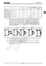
Page 203: ...Page 188 19 Package Dimensions TMP86PM29BUG ...

Page 204: ...y with version updates The recent advances in CMOS LSI production technology have been phenomenal and microcomputer systems for LSI design are constantly being improved The products described in this document may also be revised in the future Be sure to check the latest specifications before using Toshiba is developing highly integrated high performance microcomputers using advanced MOS production...

Page 205: ......

Reviews: